Three-dimensional ladar module with alignment reference insert circuitry

a three-dimensional ladar module and alignment reference technology, applied in the field of laserradar imaging technology, can solve the problems of undesirable sensor types, lack of circuit speed and capacity to achieve very high (i.e., centimeter) range resolution and sensitivity, etc., to achieve enhanced imaging capability, reduce layer-to-layer or channel-to-channel “jitter”, and increase detector output processing circuit density

Active Publication Date: 2008-10-14
NYTELL SOFTWARE LLC
View PDF8 Cites 90 Cited by
  • Summary
  • Abstract
  • Description
  • Claims
  • Application Information

AI Technical Summary

Benefits of technology

[0016]In yet a further aspect of the invention, one or more alignment reference points are inserted at a predetermined point in the image capture cycle to allow the electronic alignment of selected sets of image data collected by the FIFO shift registers in the one or more channels in one or more ROICs contained in the processing module. In this aspect of the invention, alignment reference point insertion and alignment circuitry is provided as means to minimize layer-to-layer or channel-to-channel “jitter” which may be present due to variances in layer operating or data capture start-up characteristics. Alternatively, the invention allows a user to selectively insert an alignment referen

Problems solved by technology

Unfortunately, existing LADAR imaging systems lack the necessary circuit speed and capacity to achieve very high (i.e., centimeter) range resolution and sensitivity.
Nonetheless, these types of s

Method used


Image

  • Three-dimensional ladar module with alignment reference insert circuitry
  • Three-dimensional ladar module with alignment reference insert circuitry
  • Three-dimensional ladar module with alignment reference insert circuitry

Examples


Embodiment Construction

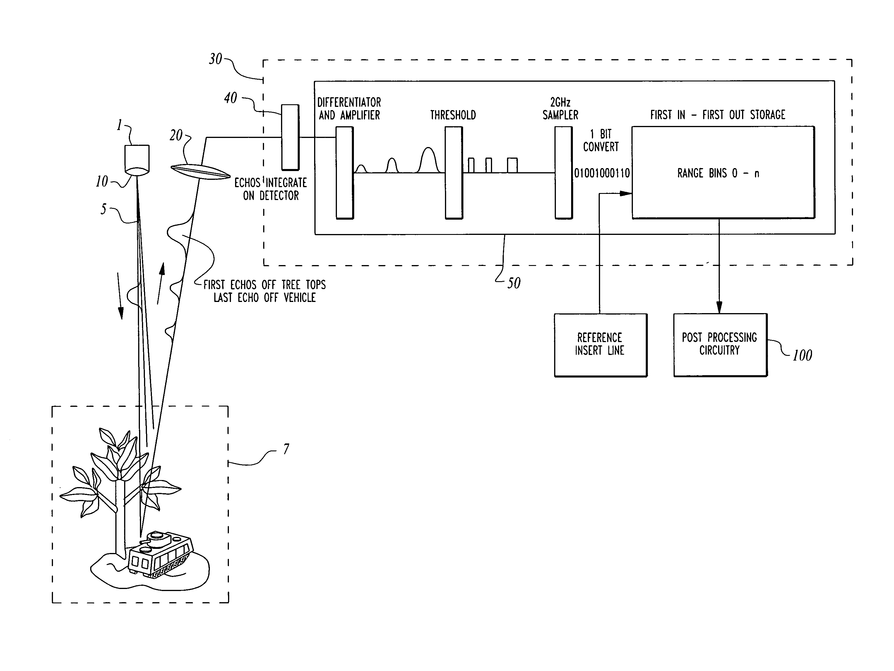
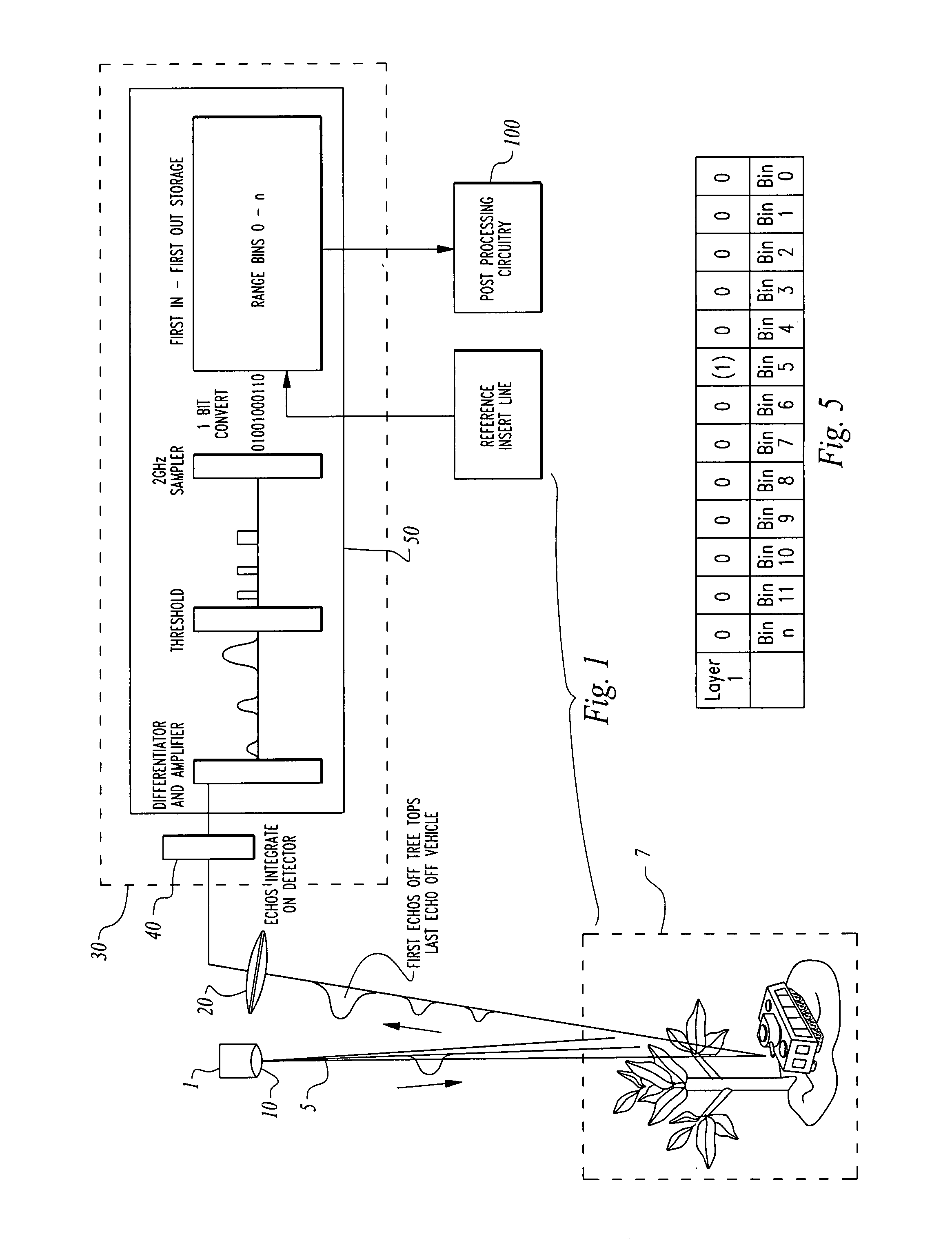
[0033]Turning now to the figures wherein like numerals designate like elements among the several views, FIG. 1 shows a block diagram of the present invention.

[0034]A photon source, such as a laser 1, generates a beam pulse 5, which is directed toward a scene or target 7, through suitable beam-shaping optics 10.

[0035]In a preferred embodiment, laser 1 is a 1064 nm, mechanically aligned, 300 micro-Joule, seed YAG laser capable of producing a pulse width of 500 picoseconds. In the preferred embodiment, a beam amplifier is provided (not shown), such as a master oscillator power amplifier, wherein a seed beam is fed into the amplifier. In this preferred embodiment, the seed beam passes through a Faraday rotator and enters a four-pass, thermally-controlled amplifier which includes two pumped YAG diodes.

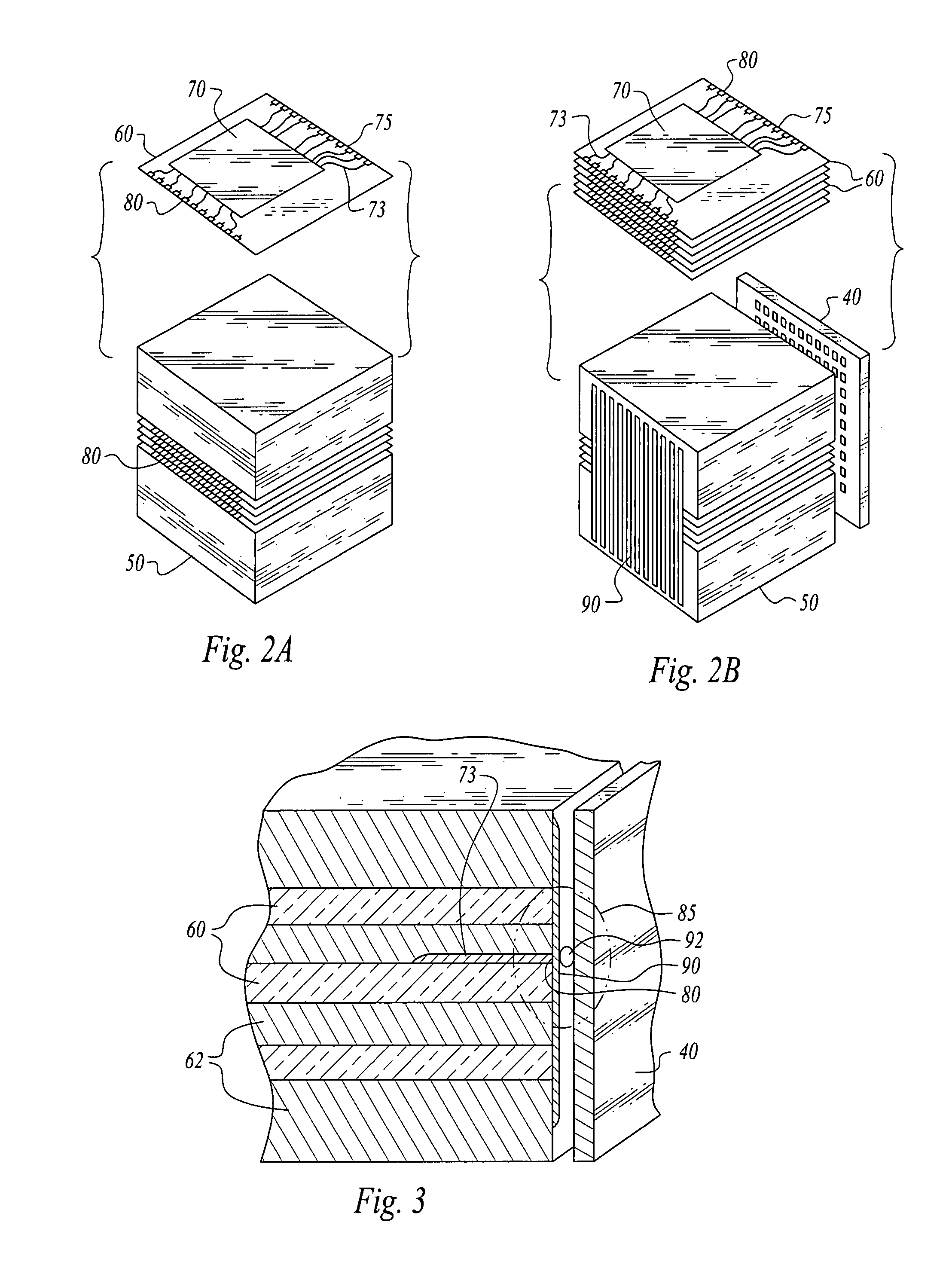
[0036]In the preferred embodiment, beam-shaping optics 10 is a beam-shaping holographic lens suitable for projecting a rectangular beam area on a target. It has been determined that a recta...


PUM


Abstract

A 3-D LADAR imaging system incorporating stacked microelectronic layers is provided. A light source such as a laser is imaged upon a target through beam shaping optics. Photons reflected from the target are collected and imaged upon a detector array though collection optics. The detector array signals are fed into a multilayer processing module wherein each layer includes detector signal processing circuitry. The detector array signals are amplified, compared to a user-defined threshold, digitized and fed into a high speed FIFO shift register range bin. Dependant on the value of the digit contained in the bins in the register, and the digit's bin location, the time of a photon reflection from a target surface can be determined. A T0 trigger signal defines the reflection time represented at each bin location by resetting appropriate circuitry to begin processing.
A reference insert circuit inserts data into the FIFO registers at a preselected location to provide a reference point at which all FIFO shift register data may be aligned to accommodate for timing differences between layers and channels. The bin data representing the photon reflections from the various target surfaces are read out of the FIFO and processed using appropriate circuitry such as a field programmable gate array to create a synchronized 3-D point cloud for creating a 3-D target image.

Description

CROSS REFERENCE TO RELATED APPLICATIONS[0001]This application is related to U.S. provisional patent application No. 60 / 785,135, filed on Mar. 24, 2006, entitled, “Method for Image Jitter Reduction in a Multilayer LADAR Device” and is a continuation-in-part of U.S. patent application Ser. No. 10 / 806,037 filed on Mar. 22, 2004, entitled, “Three-Dimensional Imaging Processing Module Incorporating Stacked Layers Containing Microelectronic Circuitry”, U.S. Pat. No. 7,180,579, issued Feb. 20, 2007 to Ludwig, et al., both of which is incorporated herein by reference and to which priority is claimed pursuant to 35 USC 119.STATEMENT REGARDING FEDERALLY SPONSORED RESEARCH AND DEVELOPMENT[0002]This invention was made with U.S. Government support under Contract No. DAAD17-01-D-0006-0002, awarded by the Army Research Laboratory (ARL). The U.S. Government has certain rights in the invention.BACKGROUND OF THE INVENTION[0003]1. Field of the Invention[0004]The instant invention relates generally to ...

Claims


Application Information

Patent Timeline
IPC IPC(8): G01C3/08
CPCG01S7/487G01S7/51G01S17/42G01S17/89G01S7/4863G01S17/894
Inventor KENNEDY, JOHNLUDWIG, DAVIDKRUTZIK, CHRISTIAN
Owner NYTELL SOFTWARE LLC
Why Eureka
Try Eureka