Method and system for forming a die frame and for transferring dies therewith

a technology of die frame and transfer die, which is applied in the field of assembly of electronic devices, can solve the problems affecting the accuracy of pick and place techniques, and reducing the accuracy of limiting the throughput volum

Inactive Publication Date: 2006-04-04
SYMBOL TECH INC
View PDF59 Cites 97 Cited by
  • Summary
  • Abstract
  • Description
  • Claims
  • Application Information

AI Technical Summary

Problems solved by technology

Pick and place techniques involve complex robotic components and control systems that handle only one die at a time.
This has a drawback of limiting throughput volume.
Furthermore, pick and place techniques have limited placement accuracy, and have a minimum die size requirement.

Method used


Image

  • Method and system for forming a die frame and for transferring dies therewith
  • Method and system for forming a die frame and for transferring dies therewith
  • Method and system for forming a die frame and for transferring dies therewith

Examples


Embodiment Construction

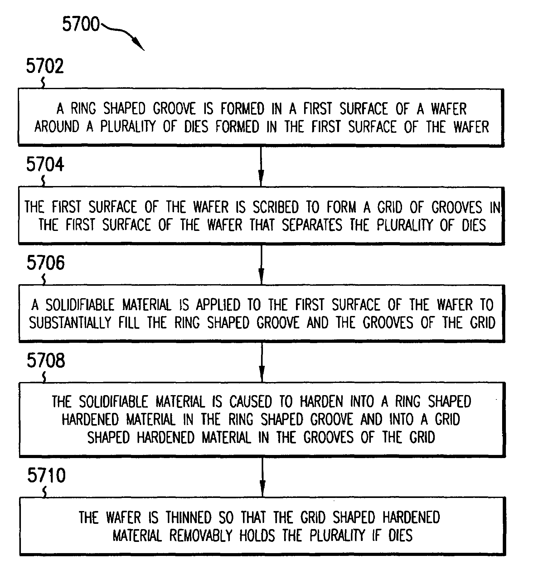
[0084]The present invention provides improved processes and systems for assembling electronic devices, including RFID tags. The present invention provides improvements over current processes. Conventional techniques include vision-based systems that pick and place dies one at a time onto substrates. The present invention can transfer multiple dies simultaneously. Vision-based systems are limited as far as the size of dies that may be handled, such as being limited to dies larger than 600 microns square. The present invention is applicable to dies 100 microns square and even smaller. Furthermore, yield is poor in conventional systems, where two or more dies may be accidentally picked up at a time, causing losses of additional dies.

[0085]The present invention provides an advantage of simplicity. Conventional die transfer tape mechanisms may be used by the present invention. Furthermore, much higher fabrication rates are possible. Current techniques process 5–8 thousand units per hour....


PUM

PropertyMeasurementUnit
thicknessesaaaaaaaaaa
thicknessaaaaaaaaaa
thicknessaaaaaaaaaa

Abstract

A method, system, and apparatus for a die frame, and for transferring integrated circuit dies therewith, is described. In one aspect for making a die frame, a wafer that comprises a plurality of dies is attached to a surface of a tape structure. A grid of grooves is formed in the wafer to separate the plurality of dies on the surface of the tape structure. A portion of the tape structure that is accessible through the grooves of the grid is caused to harden into a grid shaped structure. The grid shaped structure removably holds the plurality of dies. One or more dies of the plurality of dies can be moved from the grid shaped structure onto a target surface. In an alternative aspect, when the grid of grooves is formed in the wafer to separate the plurality of dies on the surface of the tape structure, the surface of the tape structure is breached in the grooves. The breach causes a hardening material encapsulated in the tape structure to be released and to harden in the grooves into a grid shaped hardened material.

Description

CROSS-REFERENCE TO RELATED APPLICATIONS[0001]This application claims the benefit of U.S. Provisional Application No. 60 / 400,101, filed Aug. 2, 2002, and is a continuation in part of U.S. application Ser. No. 10 / 322,701, filed Dec. 19, 2002, which are both herein incorporated by reference in their entireties.[0002]The following applications of common assignee are related to the present application, and are herein incorporated by reference in their entireties:[0003]“Method and Apparatus for High Volume Assembly of Radio Frequency Identification Tags,” Ser. No. 10 / 322,467, filed Dec. 19, 2002;[0004]“Multi-Barrel Die Transfer Apparatus and Method for Transferring Dies Therewith,” Ser. No. 10 / 322,718, filed Dec. 19, 2002; and[0005]“System and Method of Transferring Dies Using an Adhesive Surface,” Ser. No. 10 / 322,702, filed Dec. 19, 2002.BACKGROUND OF THE INVENTION[0006]1. Field of the Invention[0007]The present invention relates generally to the assembly of electronic devices. More part...

Claims


Application Information

Patent Timeline
Patent Type & Authority Patents(United States)
IPC IPC(8): G08B13/14G06K19/077H01L21/56H01L21/68H01L23/498
CPCG06K19/07718G06K19/07745G06K19/07749G06K19/0775G06K19/07758H01L21/56H01L21/563H01L21/67005H01L21/6835H01L21/6836H01L23/49855H01L23/544H01L24/96H01L24/29B29C33/06H01L24/12H01L24/28H01L24/82H01L24/83H01L24/90H01L24/97H01L2221/68313H01L2221/68327H01L2221/68354H01L2223/54426H01L2224/73203H01L2224/83191H01L2224/83851H01L2224/90H01L2924/01005H01L2924/01013H01L2924/01047H01L2924/01077H01L2924/01079H01L2924/01082H01L2924/09701H01L2924/14H01L2924/19041H01L2924/19042H01L2924/19043H01L2924/01006H01L2924/01023H01L2924/01033H01L2224/16225H01L2224/16238H01L2224/81191H01L2224/16227H01L2224/2929H01L2224/293H01L2924/00011Y10T29/4998Y10T156/10Y10T29/49474Y10T29/49016Y10T29/49117Y10T29/49885Y10T29/49279Y10T29/5313H01L2224/29075H01L2924/00014H01L2924/12042H01L2924/00
Inventor ARNESON, MICHAEL R.BANDY, WILLIAM R.
Owner SYMBOL TECH INC
Why Eureka
Try Eureka