Direct write method for polarized materials

a technology of polarized materials and write methods, applied in the direction of manufacturing tools, additive manufacturing, electric/magnetic/electromagnetic heating, etc., can solve the problems of reducing the size of the electronic packaging industry, largely limited to silicon-based materials, and the process used to fabricate the mems device still depends on expensive and complicated semiconductor equipment and facilities

Inactive Publication Date: 2003-02-13
NANOTEK INSTR GRP LLC
View PDF0 Cites 94 Cited by
  • Summary
  • Abstract
  • Description
  • Claims
  • Application Information

AI Technical Summary

Benefits of technology

0008] A direct-write method has been developed by which highly polarized materials in the form of a patterned thin film can be deposited onto a solid substrate. The materials deposited are substantially free of mechanically induced orientation and their polarization is essentially stable up to about the crystal melting point of the polarized material in the case of a crystalline material or up to about the softening point (glass transition temperature) of the polarized material in the case of non-crystalline polarized material. The method includes dissolving a material to be polarized in a solvent or solvents for that material to form a solution. The solution is then dispensed in the form of fine discrete droplets or a continuous strand in a fluent state and deposited onto a target surface in an essentially point-by-point and layer-by-layer fashion. The target may be a semiconducting substrate or a conducting electrode supported on the surface of a substrate. The solvent is selected which is adapted to the polarization of the material and which can be removed to the extent desired during the course of the polarization. A high electric field is applied to polarize the deposited material while the solvent is being removed. The temperature employed will be one at which polarization effectively occurs, normally at an elevated temperature below which substantial dielectric breakdown could occur. The DC field employed in the polarization will be selected which provides the desired polarization.
0009] Also provided by this invention is a freeform fabrication method by which a multi-layer device containing a polarized material can be produced point by point and layer by layer. Individual layers may comprise a patterned thin film of a polarized material and / or other electronically active or passive materials such as a conductor, resistor, semi-conductor, capacitor, inductor, superconductor, diode, transistor, light-emitting element, light-sensing element, solar cell element, sensor, actuator, semiconductor logic element, electro-optic logic element, spin material, magnetic material, thermo-electric element, electromagnetic wave emission, transmission or reception element, electronically addressable ink, or a combination thereof. The polarizable material presently preferred is poly (vinylidene fluoride) or certain copolymers of vinylidene fluoride. A functionally responsive device such as a micro-electro-mechanical system (MEMS) can be fabricated point by point and layer by layer under the control of a computer in accordance with a computer-aided design (CAD) of this device.

Problems solved by technology

However, the electronics packaging industry has not seen the same degree of size reduction as in the IC industry.
Many of the processes used to fabricate MEMS devices still depend on expensive and complicated semiconductor equipment and facilities, nevertheless.
These processes are largely limited to silicon-based materials.
Furthermore, some of the processing temperatures for MEMS fabrication are not compatible with electronic devices.
This is an undesirable attribute of the piezoelectric polymers.
Furthermore, the need to mechanically stretch a polymer film is not compatible with traditional microelectronics fabrication processes.
(U.S. Pat. No. 4,830,795, May 16, 1989 and No. 4,863,648, Sep. 5, 1989) disclosed a solvent polarization method to produce a thick film of a simple geometry; however, no method has been proposed that allows direct deposition of a thin film of a polarizable material with a predetermined pattern on a solid substrate.

Method used


Image

  • Direct write method for polarized materials
  • Direct write method for polarized materials
  • Direct write method for polarized materials

Examples


Embodiment Construction

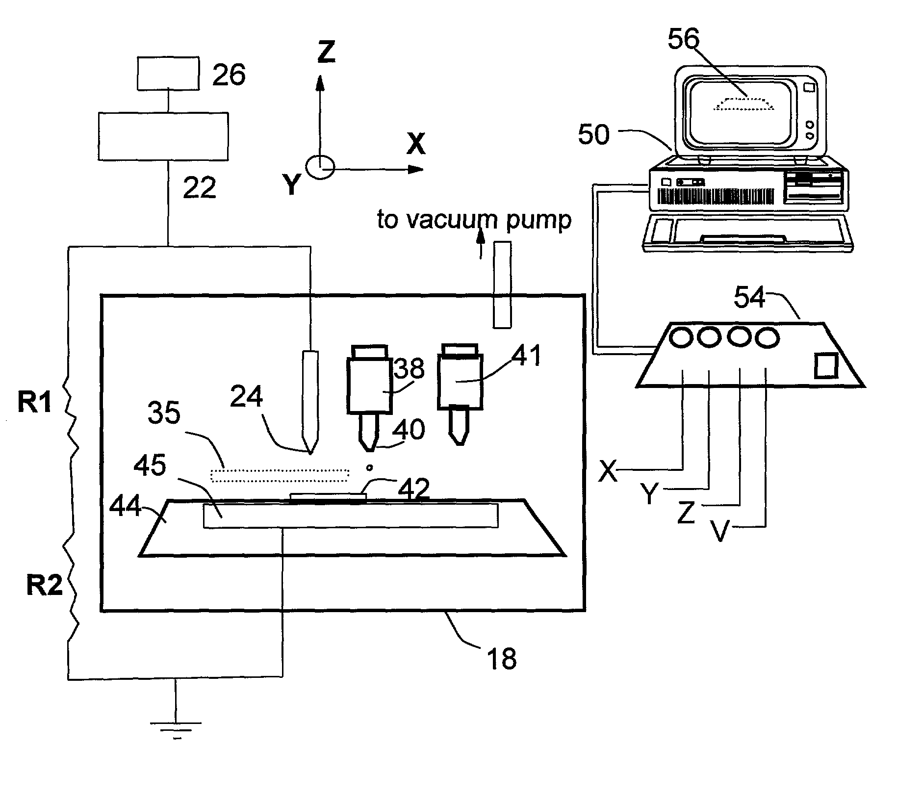
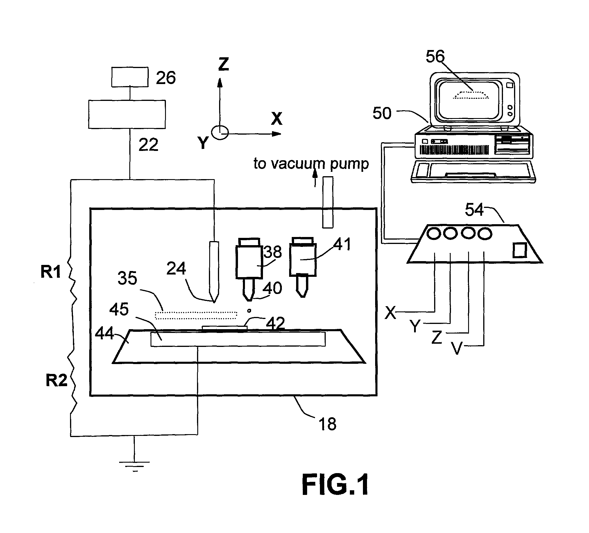
[0012] The method begins by first dissolving the material to be polarized in the required amount of a suitable solvent or solvents to form a solution. In the case of poly(vinylidene fluoride) (PVDF), a solvent such as tricresylphosphate can be used. Approximately 5% by weight of PVDF can be dissolved in 95% of tricresylphosphate or another polarization solvent for making the solution for deposition. The mixture may be heated to about 180.degree. C.-190.degree. C. to accelerate the dissolution step. A capacitor grade PVDF available from Kureha Kagoku Kogko Kabishiki Kaisha and VDF copolymer (Kynar) supplied by Pennwalt Corp. were found to be suitable.

[0013] Once a solution is prepared, it is preferred to reduce the solvent content in the solution prior to being dispensed from a dispensing device onto a target surface for polarization. For example, in the case of PVDF / tricresylphosphate solution, the solvent content can be reduced from 95% to 50% or below such as to 25% or lower provi...


PUM

PropertyMeasurementUnit
temperatureaaaaaaaaaa

Abstract

A direct-write method for depositing a polarized material of a predetermined computer-aided pattern onto a target surface, the method including the following steps: (1) forming a solution of a material capable of being polarized using a polarization solvent which can be removed by evaporation to provide a polarized material; (2) operating dispensing devices to dispense and deposit the solution onto the target surface substantially point by point and at least partially removing the solvent from the deposited solution to form a thin layer of substantially solidified material of the predetermined pattern; and (3) during the solvent-removing step, operating a high DC voltage for poling the deposited solution to achieve polarization in the material. The invention also provides a freeform fabrication method for building a multi-layer device, such as a micro-electro-mechanical system (MEMS), that exhibits piezoelectric or pyroelectric properties.

Description

[0001] This invention relates to a method for directly depositing a polarized material with a net polarization onto a substrate. This invention also provides a freeform fabrication method for making a multi-layered device that contains a polarized material which is essentially stable up to its crystal melting point (if the polarized material is crystalline) or its softening point (if the material is non-crystalline). The polarized material is substantially free of mechanically-induced orientation and has mechanical and electromechanical properties isotropic in a plane perpendicular to the poling field direction. The method is particularly useful for making a micro-electro-mechanical system (MEMS) featuring a polymeric material element with piezoelectric and pyroelectric properties.[0002] Recent advancements in the microelectronics industry have allowed integrated circuit (IC) chip manufacturer to achieve a very high packing density within a single IC chip. However, the electronics p...

Claims


Application Information

Patent Timeline
Patent Type & Authority Applications(United States)
IPC IPC(8): B29C67/00H01L41/45
CPCB29C67/0059B29C67/0092B29K2995/0073H01L41/257H01L41/45B29C64/112B29C64/40B33Y10/00B33Y40/20H10N30/045H10N30/077H10N30/098
Inventor HUANG, WEN-CHIANG
Owner NANOTEK INSTR GRP LLC
Why Eureka
Try Eureka