Structure and method for realizing physical consolidation of pixels

A technology of pixels and pixel units, applied in image communication, components of color TVs, components of TV systems, etc., can solve the problems of improving noise, low illumination, and unsatisfactory results, and achieve the effect of reducing errors

Active Publication Date: 2015-04-01
SHANGHAI INTEGRATED CIRCUIT RES & DEV CENT +1
View PDF3 Cites 12 Cited by
  • Summary
  • Abstract
  • Description
  • Claims
  • Application Information

AI Technical Summary

Problems solved by technology

[0009] The effects of these solutions, either improve the low-light performance while increasing the noise, or ne

Method used


Image

  • Structure and method for realizing physical consolidation of pixels
  • Structure and method for realizing physical consolidation of pixels
  • Structure and method for realizing physical consolidation of pixels

Examples


Embodiment Construction

[0058] In order to make the content of the present invention clearer and easier to understand, the content of the present invention will be further described below in conjunction with the accompanying drawings. Of course, the present invention is not limited to this specific embodiment, and general replacements known to those skilled in the art are also covered within the protection scope of the present invention.

[0059] Secondly, the present invention is described in detail by means of schematic diagrams. When describing the examples of the present invention in detail, for the convenience of explanation, the schematic diagrams are not partially enlarged according to the general scale, which should not be used as a limitation of the present invention.

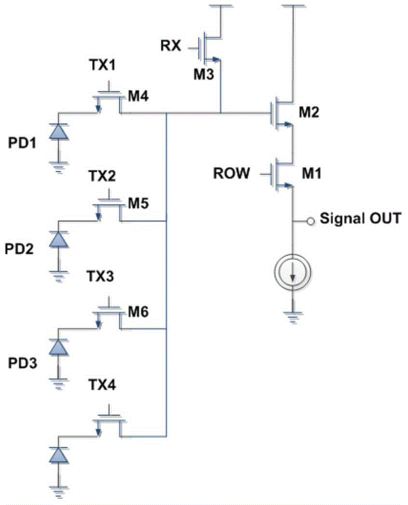
[0060] This solution uses a 1.75T 4-in-1 pixel unit circuit, such as image 3 As shown, the circuit consists of the following basic components:

[0061] 1) 4 photodiodes, i.e. 4 pixels

[0062] 2) Readout switching transist...


PUM


Abstract

The invention provides an image sensor structure for realizing physical consolidation of pixels. The image sensor structure comprises a pixel unit circuit array and filters, the filters cover all pixels in the array, and the array is formed by combining and extending multiple red, blue and green pixel unit circuits which meet the minimum BAYER pattern. Each pixel unit circuit comprises four pixels, one pixel unit circuit is only covered by the filter in one color, and the pixel unit circuits are arranged at intervals according to the minimum square array. The invention also provides a method for realizing physical consolidation of the pixels. By controlling peripheral circuits in the pixel unit circuits, signals of every four pixels are read at the same time, and physical consolidation is completed. The structure and method realize direct consolidation of photoelectrons through physical consolidation, errors caused by introduction of digital-to-analogue conversion are avoided, special data algorithms and complex peripheral circuits are not needed, and the sizes of the pixel units can be further reduced conveniently through a new framework with transistor pixels shared.

Description

technical field [0001] The invention relates to the field of CMOS image sensors, in particular to a structure and method for realizing physical combination of pixels. Background technique [0002] The image sensor is an important part of the camera. In traditional cameras, the image sensor is realized by film, while in modern digital cameras, the image sensor is realized by CMOS or CCD image sensor. [0003] The pixel unit of a CMOS image sensor is the core device of the image sensor to realize light sensing. It usually includes: a photodiode of the photosensitive unit to realize photoelectric conversion and a series of transistors that transmit, convert, amplify and control the signal of the photosensitive unit. Traditional CMOS image sensors use 3 to 4 transistors per pixel. [0004] With more and more mobile devices equipped with cameras, CMOS imaging technology for embedded applications is developing rapidly. For a pixel unit, if the area of ​​the pixel unit is larger...

Claims


Application Information

Patent Timeline
IPC IPC(8): H04N9/04H04N5/378
Inventor 雷冬梅
Owner SHANGHAI INTEGRATED CIRCUIT RES & DEV CENT
Why Eureka
Try Eureka