LED device with transition substrate and packaging method thereof

A technology for LED devices and transition substrates is applied in the field of LED devices with transition substrates and their packaging, which can solve the problems of limitation, high cost, and inability to produce devices, and achieve the effects of low cost, reduced stress, and high chip reliability.

Active Publication Date: 2017-08-08
FOSHAN NATIONSTAR OPTOELECTRONICS CO LTD
View PDF8 Cites 0 Cited by
  • Summary
  • Abstract
  • Description
  • Claims
  • Application Information

AI Technical Summary

Problems solved by technology

However, on the one hand, the cost of the ceramic substrate is much higher than that of the metal substrate. On the other hand, because the ceramic substrate itself is relatively brittle, especially for large-area packaged or strip-packaged COB devices, the flip-chip LED chip ceramic substrate COB devices are also limited and cannot produce devices of any shape and size

Method used


Image

  • LED device with transition substrate and packaging method thereof
  • LED device with transition substrate and packaging method thereof
  • LED device with transition substrate and packaging method thereof

Examples


Embodiment Construction

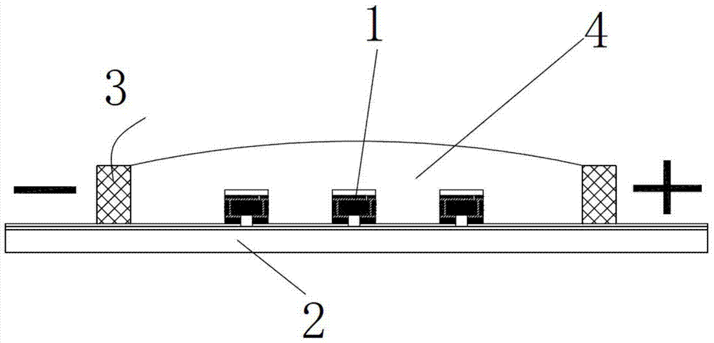
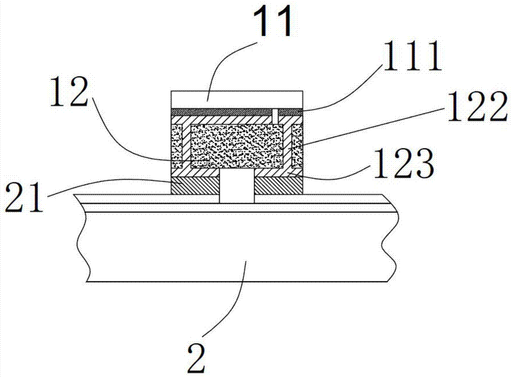
[0041] Please also see figure 1 and figure 2 ,in, figure 1It is a cross-sectional structural schematic diagram of an LED device with a transition substrate in the present invention, figure 2 yes figure 1 The shown schematic diagram of the cross-sectional structure of the LED unit arranged on the metal substrate.

[0042] Such as figure 1 As shown, the LED COB device with a transition substrate of the present invention includes: at least one LED unit 1 , a metal substrate 2 , a dam 3 and an encapsulant (not shown in the figure). The LED unit 1 is welded on the metal substrate 2 and electrically connected thereto. The dam 3 is arranged on the edge of the metal substrate 2 and surrounds all the LED units 1 on the metal substrate to form an enclosing area 4 for packaging. The encapsulant is filled in the surrounding area 4 and covers and seals all the LED units 1 inside.

[0043] Specifically, such as figure 2 As shown, the LED unit 1 includes an LED chip 11 and a trans...


PUM


Abstract

An LED device with transition substrates comprises at least one LED unit, a metal substrate and packaging rubber. Each LED unit comprises an LED chip and a transition substrate, expansion coefficient of each transition substrate is between the expansion coefficients of the LED chips and the metal substrate, and the difference of the expansion coefficients of the LED chips is 0-20% of the expansion coefficient of the LED chips. The LED chips are flip chips and provided with positive and negative electrodes at the bottoms. The upper surface of each transition substrate is provided with at least two welding layers which are insulated to each other. The lower surface of each transition substrate is provided with at least two surface-mounted pins which are insulated. The welding layers are electrically connected with the surface-mounted pins. The positive and negative electrodes of the LED chips are connected with the welding layers of the transition substrates respectively so as to form the LED units, the LED units are arranged on the metal substrate through the surface-mounted pins of the transition substrates, and the packaging rubber covers and packages the LED units. The LED COB (chip on board) device is high in reliability and low in production cost, and shape and size of the LED COB device are not limited.

Description

technical field [0001] The invention relates to the field of LED packaging, in particular to an LED device with a transition substrate and a packaging method thereof. Background technique [0002] With the development of LED packaging in the direction of thinner and lower cost, chip-on-board (COB) packaging technology is gradually emerging. The production cost, brightness and reliability of LEDCOB devices are all important indicators to measure the quality of LEDCOB devices. Therefore, people have been working on improving the reliability of LEDCOB devices and reducing production costs. [0003] In order to improve the brightness and reliability of LEDCOB devices and reduce production costs, the existing technologies mainly include: [0004] 1. COB devices with LED chip metal substrates: In order to improve the brightness of COB devices and have a good heat dissipation effect, multiple LED chips are usually mounted on the metal substrate, and gold wires are used to realize...

Claims


Application Information

Patent Timeline
Patent Type & Authority Patents(China)
IPC IPC(8): H01L33/48H01L33/62H01L25/075
CPCH01L33/005H01L33/48H01L33/62H01L2933/0033H01L2933/0066
Inventor 李宗涛丁鑫锐李宏浩关沃欢
Owner FOSHAN NATIONSTAR OPTOELECTRONICS CO LTD
Why Eureka
Try Eureka