Circuit board jig and ink hole-plugging method

A technology for circuit boards and printed circuit boards, which is applied in the directions of printed circuits, printed circuit manufacturing, mechanical/acoustic circuit processing, etc., can solve the problems of poor plugging ink fullness, poor ink plugging effect, and low product qualification rate. To achieve the effect of good plumpness, improved applicability and high product qualification rate

Inactive Publication Date: 2015-04-15
SHENZHEN WUZHU TECH
View PDF3 Cites 9 Cited by
  • Summary
  • Abstract
  • Description
  • Claims
  • Application Information

AI Technical Summary

Problems solved by technology

[0005] In order to solve the technical problems of the above circuit board plugging method, such as complicated process, poor ink plugging effect, poor plugging ink plumpness and low product qualification rate, the present invention provides a plugging ink with simple process and good ink plugging effect. The ink plugging method with good plumpness and high product qualification rate; the present invention also provides a circuit board jig for realizing the ink plugging method

Method used


Image

  • Circuit board jig and ink hole-plugging method
  • Circuit board jig and ink hole-plugging method

Examples


Embodiment Construction

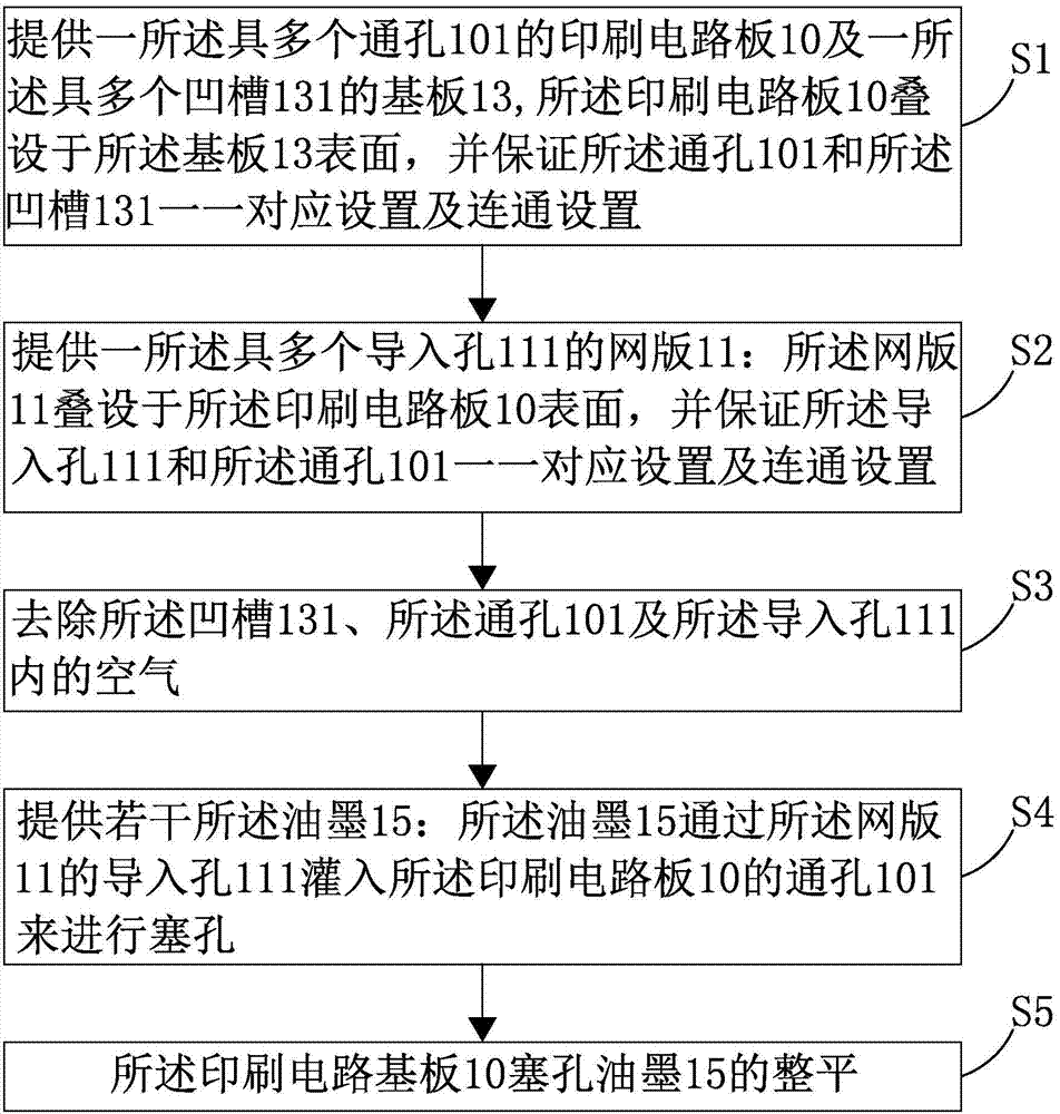
[0037] The following will clearly and completely describe the technical solutions in the embodiments of the present invention with reference to the accompanying drawings in the embodiments of the present invention. Obviously, the described embodiments are only part of the embodiments of the present invention, not all of them. Based on the embodiments of the present invention, all other embodiments obtained by persons of ordinary skill in the art without making creative efforts belong to the protection scope of the present invention.

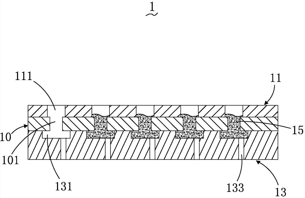
[0038] see figure 1 , is a structural schematic diagram of the circuit board jig provided by the present invention. The circuit board jig 1 is used to make ink plug holes in the printed circuit board 10 having a plurality of through holes 101 . The circuit board fixture 1 includes a screen 11 , a substrate 13 and a plurality of inks 15 .

[0039] The screen 11 is an aluminum screen, its size is greater than or equal to the size of the printed c...


PUM


Abstract

The invention relates to a circuit board jig which is used for performing ink hole-plugging on a printed circuit board with multiple through holes. The circuit board jig comprises a screen printing plate, a baseboard and a lot of ink, the screen printing plate comprises multiple guide-in holes formed in a manner of penetrating the surface of the screen printing plate, the baseboard comprises multiple grooves formed in the surface of the baseboard, the screen printing plate is arranged on the surface of the printed circuit board, the guide-in holes, the through holes and the grooves are arranged in a one-to-one corresponding manner and in a mutually communicated manner, and the through holes are filled with the ink. The invention further relates to an ink hole-plugging method utilizing the circuit board jig.

Description

technical field [0001] The invention relates to the technical field of circuit board production, in particular to a circuit board jig and an ink plugging method. Background technique [0002] With the improvement and progress of printed circuit board assembly requirements, more and more printed circuit boards require plug holes. The ink plugging process of printed circuit boards is a special process using screen printing developed with surface mount technology. In addition to providing solder mask patterns and surface protection circuits, it also provides convenience for surface mount processes. [0003] The purpose of the ink plug hole is mainly: in the various through holes of the printed circuit board, except for the component insertion hole, installation hole, heat dissipation hole or test hole, the other via holes do not need to be exposed, and the ink plug hole can prevent subsequent Flux or solder penetrates from the soldering surface to the component surface through...

Claims


Application Information

Patent Timeline
Patent Type & Authority Applications(China)
IPC IPC(8): H05K3/00H05K3/40
CPCH05K3/4038H05K2203/02
Inventor 徐学军赵南清
Owner SHENZHEN WUZHU TECH
Why Eureka
Try Eureka