Assembly process method for 3D Plus encapsulating device

A technology for packaging devices and assembly processes, which is applied in the direction of electrical components, assembling printed circuits with electrical components, and manufacturing printed circuits. It can solve problems such as not meeting standard requirements and no solder infiltration of device pins, and achieve good solder joint consistency. , Improve the effect of capillary action, the effect of stable and reliable device assembly quality

Active Publication Date: 2015-04-22
10TH RES INST OF CETC
View PDF4 Cites 14 Cited by
  • Summary
  • Abstract
  • Description
  • Claims
  • Application Information

AI Technical Summary

Problems solved by technology

[0005] The present invention aims at the assembly difficulties of the above-mentioned 3D PLUS packaged devices and the shortcomings of the existing assembly technology, and provides a simple, efficient, and s

Method used


Image

  • Assembly process method for 3D Plus encapsulating device

Examples


Embodiment Construction

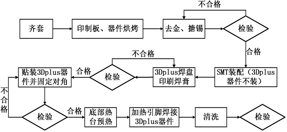
[0015] refer to figure 1 . In the invention of the 3D PLUS packaged device assembly process, the 3D PLUS packaged device complete set, printed board / device baking, gold removal, and tinning treatment process are the same as the current manual assembly process, the difference is that This assembly technology first uses the printing and patch technology in the SMT assembly technology to print the solder paste on the printed board pad with the stencil and complete the 3D PLUS packaging device placement, and controls the printed board soldering through the thickness of the stencil. The thickness of the solder paste printed on the disk is 0.12mm. Use the maintenance workstation to complete the mounting of 3D PLUS packaged devices. The lateral offset of the 3D PLUS packaged device pins is controlled within 15% of the pin width. After mounting, it is fixed with a soldering iron spot welding 3D PLUS packaged device diagonal pins; secondly, use the hot stage welding technology and too...


PUM

PropertyMeasurementUnit
Thicknessaaaaaaaaaa
Thicknessaaaaaaaaaa

Abstract

The invention discloses an assembly process method for a 3D PLUS encapsulating device, and aims to provide an assembly method, which is simple and efficient and contributes to the realization of stable and reliable quality in order to solve the problems of freeness from soldering tin infiltration on the root part of a device pin and failure in meeting certain standards caused by current manual assembly. According to the technical scheme, the method comprises the following steps: printing soldering paste on a printed board bonding pad by using a steel mesh and finishing device mounting through printing and mounting technologies in an SMT (Surface Mount Technology) assembly technology, printing the soldering paste on the printed board bonding pad, controlling the thickness of the soldering paste printed on the printed board bonding pad at 0.12 millimeter through the thickness of the steel mesh, finishing device mounting by using a maintenance workstation, controlling the lateral deviation of the device pin within 15 percent of the pin width, and fixing diagonal pins of the 3D PLUS encapsulating device through spot welding by using soldering iron after mounting; performing non-contact integral board preheating on the bottom of the printed board by using a heating stage welding technology and a tool gasket; and after preheating time is reached, manually heating the exposed pins of the device by using the soldering iron, and melting the soldering tin through thermal conduction to finish welding.

Description

technical field [0001] The invention relates to an electronic assembly process method for 3D PLUS packaging devices commonly used in products in the aerospace field. Background technique [0002] In high-reliability fields such as aerospace and military, the quality of electronic packaging is an important factor affecting the reliability of the system, and the key to the reliability of electronic packaging is the fatigue failure of solder joints. As an aerospace-grade fine-pitch device, 3D PLUS plays an important role in satellite electronic systems. It uses three-dimensional (3D) packaging technology. Compared with traditional surface mount devices, 3D PLUS packaging devices have a larger Z-direction size, The center of gravity is high, and its special packaging process brings many technical difficulties such as lead tinning, welding and protection. 3D packaging technology refers to the 3D high-density microelectronic packaging technology formed by the further development ...

Claims


Application Information

Patent Timeline
IPC IPC(8): H05K3/34
CPCH05K3/3494H05K2203/043
Inventor 吴军
Owner 10TH RES INST OF CETC
Why Eureka
Try Eureka