A Tunneling Field Effect Transistor with Electric Field Concentration Effect Enhanced On-state Current

A tunneling field effect, on-state current technology, applied in circuits, electrical components, semiconductor devices, etc., can solve the problems of increasing the static power consumption of the device, increasing the on-state current of the device, and increasing the off-state current of the device, etc. Achieve the effect of reducing the tunneling distance and the energy band bending is steep

Active Publication Date: 2018-01-12
UNIV OF ELECTRONICS SCI & TECH OF CHINA
View PDF3 Cites 0 Cited by
  • Summary
  • Abstract
  • Description
  • Claims
  • Application Information

AI Technical Summary

Problems solved by technology

However, the narrow bandgap material increases the off-state current of the device while increasing the on-state current of the device, which increases the static power consumption of the device.

Method used


Image

  • A Tunneling Field Effect Transistor with Electric Field Concentration Effect Enhanced On-state Current
  • A Tunneling Field Effect Transistor with Electric Field Concentration Effect Enhanced On-state Current
  • A Tunneling Field Effect Transistor with Electric Field Concentration Effect Enhanced On-state Current

Examples


Embodiment

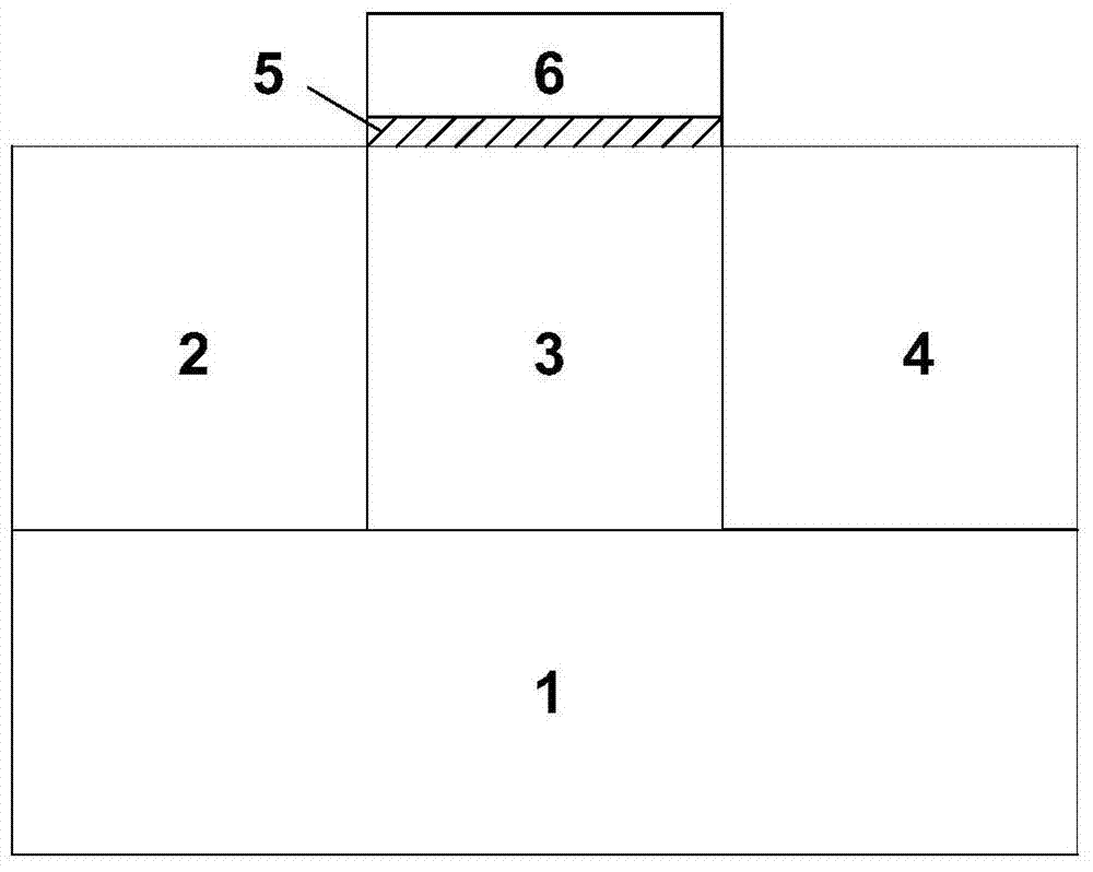
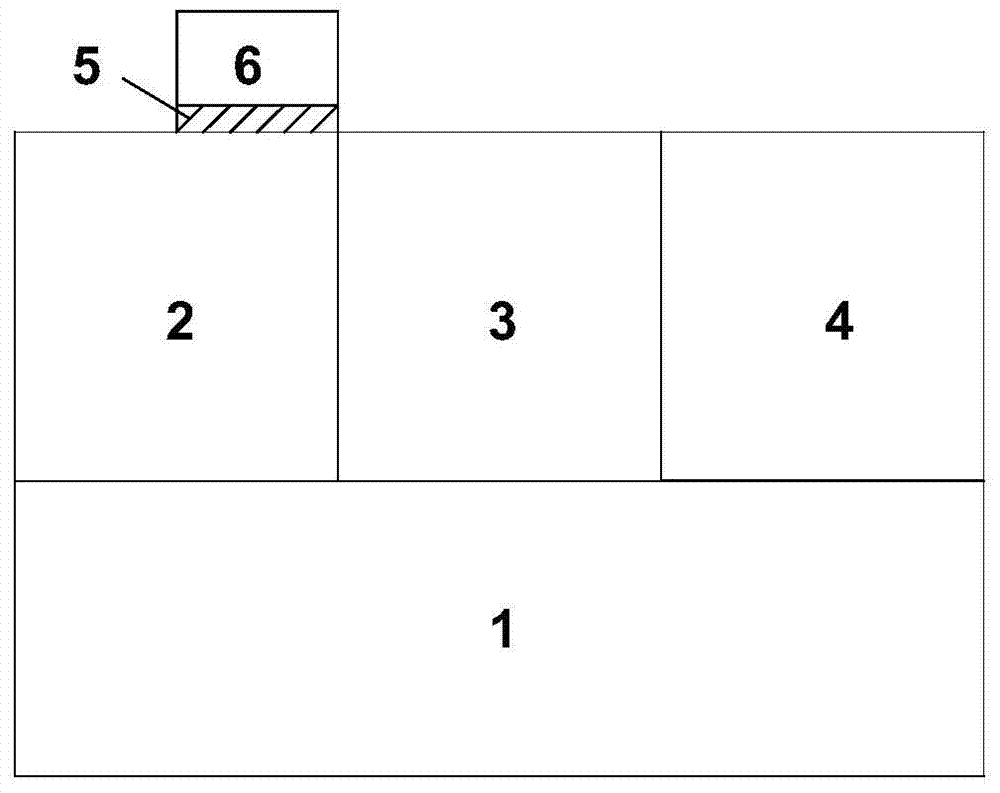
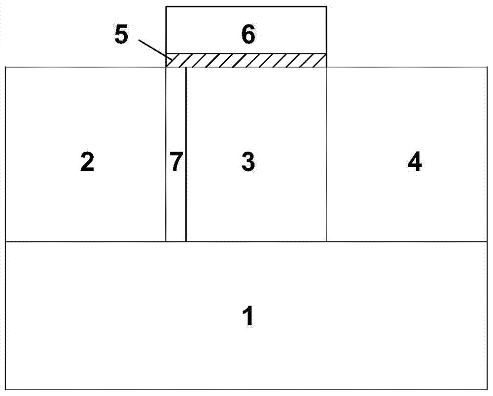
[0044] A vertical tunneling field effect transistor with a low dielectric constant dielectric block, the cross-sectional view of the transistor is shown in Figure 6 As shown, it includes a semiconductor substrate 1, a source region 2, an intrinsic region 3 and a drain region 4 formed on the semiconductor substrate 1, the intrinsic region is located between the source region and the drain region, part of the source region is above and There is also an epitaxial intrinsic region above the intrinsic region, a gate oxide layer 5 and a metal gate 6 are above the epitaxial intrinsic region above part of the source region, and the two sides of the gate oxide layer 5 and the metal gate 6 are sidewalls 9 , characterized in that it also includes a dielectric block located in the intrinsic region, on the interface between the intrinsic region and the source region, the upper surface of the dielectric block is flush with the upper surface of the source region, and the cross section of the...


PUM


Abstract

The invention provides a tunneling field effect transistor with an electric field concentration effect to enhance the on-state current, which belongs to the field of semiconductor devices. The Tunneling Field Effect Transistor with electric field concentration effect to enhance the on-state current of the present invention includes a semiconductor substrate 1, a source region 2, an intrinsic region 3, a drain region 4, a gate oxide layer 5, a metal gate 6, and sidewalls 9, and further includes The dielectric block 10 located in the intrinsic region, the dielectric block 10 is arranged on the interface between the intrinsic region and the source region, the dielectric block can change the electric field distribution at the tunnel junction position, making the electric field lines at the tunnel junction more concentration, thereby increasing the on-state current.

Description

technical field [0001] The invention belongs to the field of semiconductor devices, and in particular relates to a structure of a tunneling field effect transistor (TFET) which has an electric field concentration effect to enhance an on-state current. Background technique [0002] As the feature size of the traditional MOSFET (Metal Oxide Semiconductor Field Effect Transistor, Metal-Oxide-Semiconductor Field Effect Transistor) continues to shrink, the short-channel effect of the device becomes more and more serious, and the leakage current of the device increases, which makes the device The ratio of the on-state current to the off-state current of the device (that is, the switching ratio Ion / Ioff) continues to decrease, and the problem of power consumption is becoming more and more serious. In order to solve this problem, people began to look for new devices to replace MOSFETs. [0003] TFET (Tunneling Field Effect Transistor, tunneling field effect) transistor is a quantum...

Claims


Application Information

Patent Timeline
Patent Type & Authority Patents(China)
IPC IPC(8): H01L29/739H01L29/06
CPCH01L29/0607H01L29/78
Inventor 王向展刘葳张易孙占杰曹建强于奇
Owner UNIV OF ELECTRONICS SCI & TECH OF CHINA
Why Eureka
Try Eureka