Tunneling field-effect transistor with composite-mechanism strip-type grid and preparation method of tunneling field-effect transistor

A tunneling field effect and transistor technology, which is applied in the manufacture of diodes, semiconductor devices, semiconductor/solid-state devices, etc., can solve the problems of TFET subthreshold slope degradation, limit the application of TFET devices, and the electric field at the tunnel junction is not large enough, etc., to achieve Effect of suppressing short channel effect, improving subthreshold slope, and suppressing bulk leakage current

Active Publication Date: 2013-12-25
PEKING UNIV
View PDF4 Cites 4 Cited by
  • Summary
  • Abstract
  • Description
  • Claims
  • Application Information

AI Technical Summary

Problems solved by technology

TFET has many excellent characteristics such as low leakage current, low subthreshold slope, low operating voltage, and low power consumption. However, due to the limitation of source junction tunneling probability and tunneling area, TFET faces the problem of small on-state current, far It is not as good as traditional MOSFET devices, which greatly limits the application of TFET devices
In addition, TFET devices with a steep subthreshold slope are also difficult to realize experimentally, because it is difficult to achieve a steep doping concentration gradient at the source junction so that the electric field at the tunnel junction is not large enough when the device is turned on. This causes the subthreshold slope of the TFET to degrade from the theoretical value

Method used


Image

  • Tunneling field-effect transistor with composite-mechanism strip-type grid and preparation method of tunneling field-effect transistor
  • Tunneling field-effect transistor with composite-mechanism strip-type grid and preparation method of tunneling field-effect transistor
  • Tunneling field-effect transistor with composite-mechanism strip-type grid and preparation method of tunneling field-effect transistor

Examples


Embodiment Construction

[0032] The present invention will be further described below by example. It should be noted that the purpose of the disclosed embodiments is to help further understand the present invention, but those skilled in the art can understand that various replacements and modifications are possible without departing from the spirit and scope of the present invention and the appended claims of. Therefore, the present invention should not be limited to the content disclosed in the embodiments, and the protection scope of the present invention is subject to the scope defined in the claims.

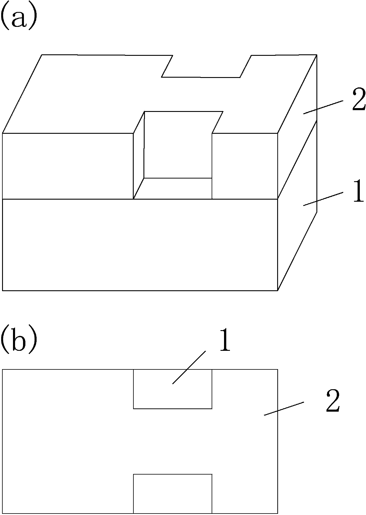
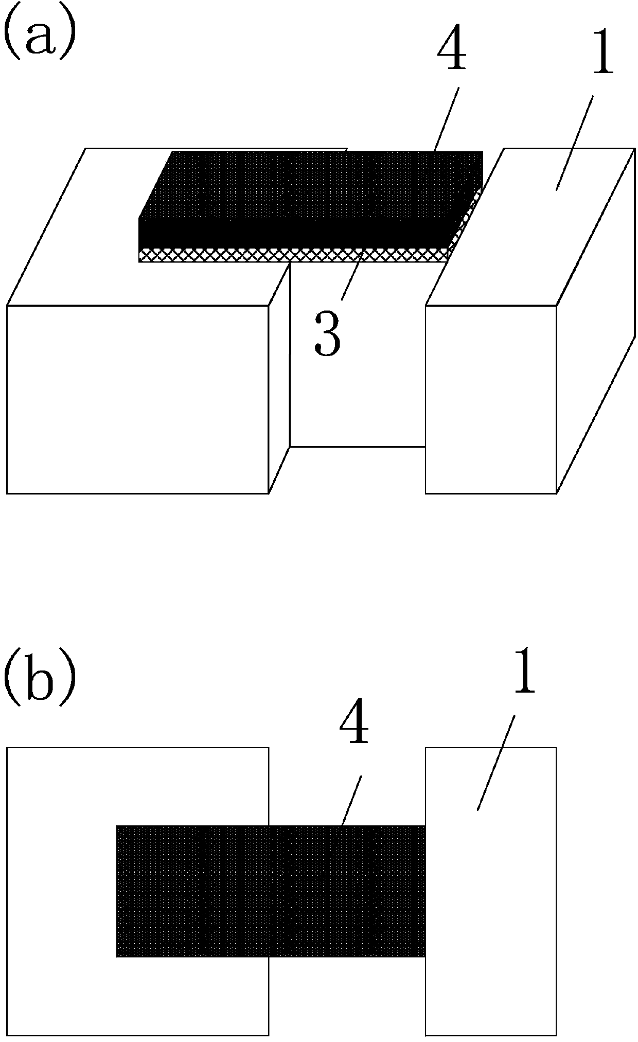
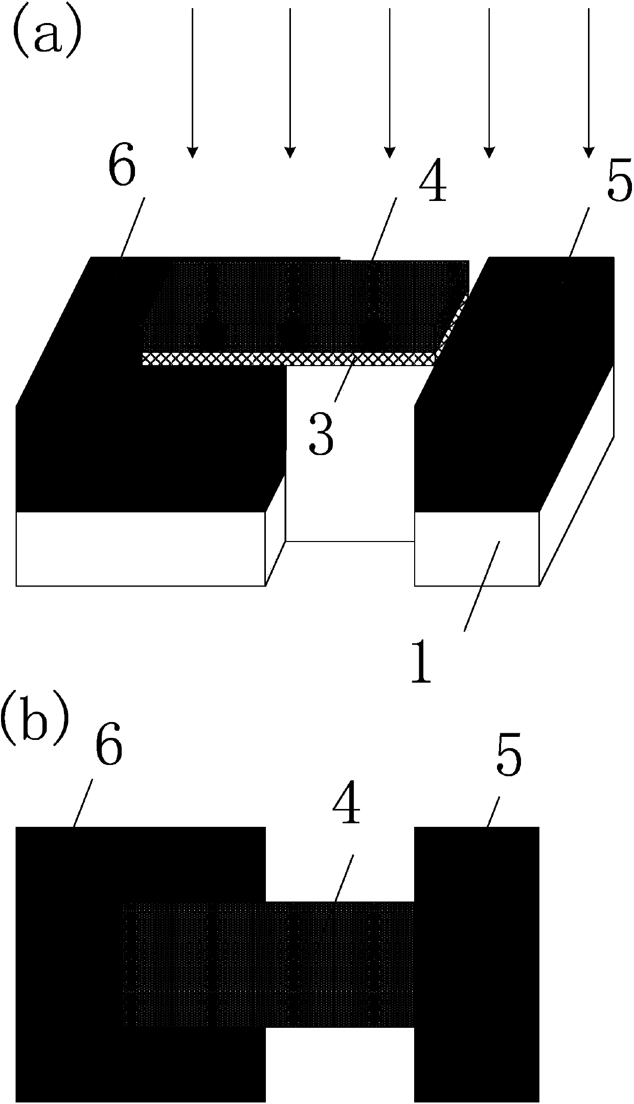
[0033] A specific example of the preparation method of the present invention includes Figure 1 to Figure 5 Process steps shown:

[0034] 1. Select a bulk silicon wafer silicon substrate 1 with a crystal orientation of (1007), the doping concentration of the substrate is lightly doped, and photo-etch the active region pattern of the word "工" on it, as shown in figure 1 (a), figure 1 As shown in...


PUM


Abstract

The invention discloses a tunneling field-effect transistor with a composite-mechanism strip-type grid and a preparation method of the tunneling field-effect transistor and belongs to the field of logic devices and circuits of field-effect transistors in CMOS (Complementary Metal Oxide Semiconductor) ultra-large-scale integrated (ULSI) circuits. The tunneling field-effect transistor has the advantages that the energy band of surface channels under the grid can be improved by changing the shape of the grid and utilizing a depletion effect of PN nodes on the two sides of the strip-type grid, and the subthreshold characteristic of the device is improved; since a composite mechanism is introduced into double-doped source areas, an ON state current of the device is improved; due to an I-shaped design of an active area, body leakage currents, including a source-drain direct tunneling current and a punching current, between the two doped source areas to a doped drain area can be greatly inhibited, and a short-channel effect is inhibited, so that the device with small size can be applied.

Description

technical field [0001] The invention belongs to the field of field effect transistor logic devices and circuits in CMOS ultra large integrated circuits (ULSI), and in particular relates to a bar-shaped gate tunneling field effect transistor with a compound mechanism and a preparation method thereof. Background technique [0002] Driven by Moore's Law, the feature size of traditional MOSFETs continues to shrink, and has now entered the nanometer scale. Following this, negative effects such as the short-channel effect of the device have become more serious. The leakage-induced barrier reduction, band-band tunneling and other effects make the off-state leakage current of the device continuously increase. At the same time, the sub-threshold slope of the traditional MOSFET is limited by the thermoelectric potential and cannot be reduced synchronously with the shrinking of the device size, thus increasing device power consumption. The power consumption problem has become the most...

Claims


Application Information

Patent Timeline
Patent Type & Authority Applications(China)
IPC IPC(8): H01L29/78H01L29/417H01L29/423H01L29/08H01L21/336
CPCH01L29/7391H01L21/0415H01L29/66356H01L29/0865H01L29/1033H01L29/41775H01L29/66492H01L29/7833
Inventor 黄如黄芊芊吴春蕾王佳鑫詹瞻王阳元
Owner PEKING UNIV
Why Eureka
Try Eureka