Radio-frequency LDMOS (laterally diffused metal oxide semiconductor) device and manufacturing method thereof

A manufacturing method and device technology, applied in semiconductor/solid-state device manufacturing, semiconductor devices, electrical components, etc., can solve problems such as failure and breakdown

A manufacturing method and device technology, applied in semiconductor/solid-state device manufacturing, semiconductor devices, electrical components, etc., can solve problems such as failure and breakdown

CN104576731AActive Publication Date: 2015-04-29SHANGHAI HUAHONG GRACE SEMICON MFG CORP

Image

  • Radio-frequency LDMOS (laterally diffused metal oxide semiconductor) device and manufacturing method thereof
  • Radio-frequency LDMOS (laterally diffused metal oxide semiconductor) device and manufacturing method thereof
  • Radio-frequency LDMOS (laterally diffused metal oxide semiconductor) device and manufacturing method thereof

Examples


Embodiment Construction

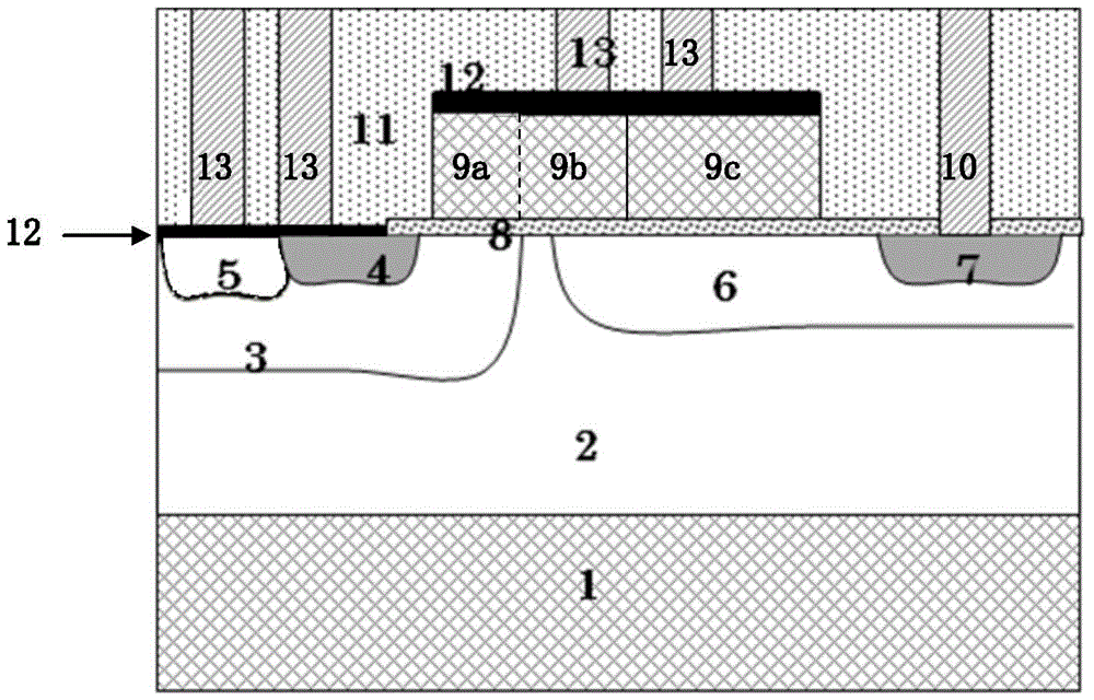
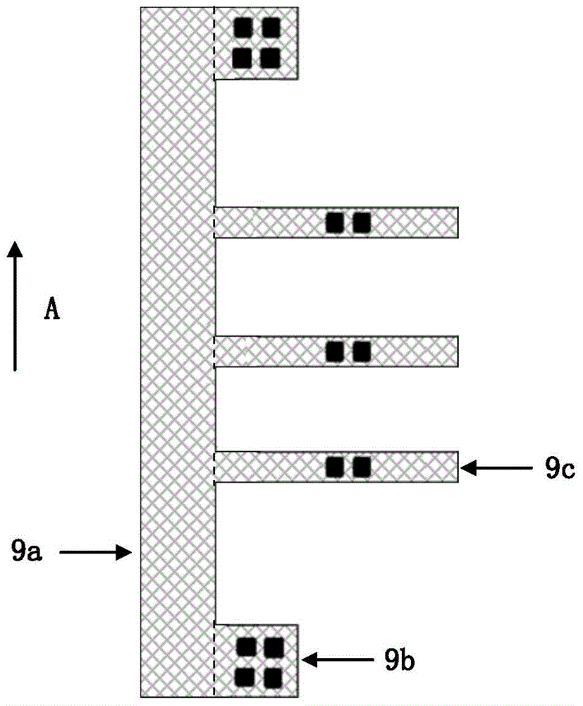
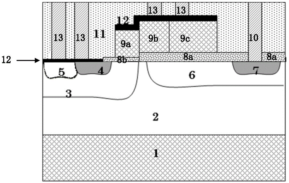
[0028] see figure 2 , which is the RF LDMOS device of this application. There is a lightly doped p-type epitaxial layer 2 on a heavily doped p-type substrate 1 . In the epitaxial layer 2 there is a p-type body region 3 and an n-type drift region 6, the sides of which may or may not be in contact. The body region 3 has a heavily doped n-type source region 4 and a heavily doped p-type body region lead-out region 5, and the sides of the two are in contact. The body region lead-out region 5 is used to lead the body region 3 out. In the drift region 6 there is a heavily doped n-type drain region 7 . There is a pad oxide layer 8a extending from the drift region 6 to the drain region 7, or part of the epitaxial layer 2 extending to the drain region 7 (depending on whether the side of the body region 3 and the drift region 6 are in contact or not). . On part of the source region 4 and part of the body region 3, or on part of the source region 4 and part of the body region 3 and ...


PUM


Abstract

The invention discloses a radio-frequency LDMOS (laterally diffused metal oxide semiconductor) device. A semiconductor region and a drift region are arranged in an epitaxial layer; a source region is arranged in the semiconductor region; a drain region is arranged in the drift region; a liner oxidation layer is arranged above part of the drift region or above part of the drift region and part of the epitaxial layer; a grid oxidation layer is arranged above part of the source region and part of the semiconductor region or above part of the source region, part of the semiconductor region and part of the epitaxial layer; the liner oxidation layer is thicker than the grid oxidation layer; a polycrystalline silicon grid is arranged above the liner oxidation layer and the grid oxidation layer; the grid consists of a main body, a first extension part and a second extension part; the main body of the grid is only located above the grid oxidation layer, and both the extension parts of the grid are only located above the liner oxidation layer. The invention further discloses a manufacturing method of the radio-frequency LDMOS device. With the adoption of the radio-frequency LDMOS device and the manufacturing method thereof, the reliability of the grid can be improved, the IGSS failure is eliminated, and the yield of the devices is increased.

Description

technical field [0001] The present application relates to a semiconductor integrated circuit device, in particular to a radio frequency LDMOS (Laterally Diffused MOS Transistor) device. Background technique [0002] see figure 1 , which is an existing RF LDMOS device. There is a lightly doped p-type epitaxial layer 2 on a heavily doped p-type substrate 1 . In the epitaxial layer 2 there is a p-type body region 3 and an n-type drift region 6, the sides of which may or may not be in contact. The body region 3 has a heavily doped n-type source region 4 and a heavily doped p-type body region lead-out region 5, and the sides of the two are in contact. The body region lead-out region 5 is used to lead the body region 3 out. In the drift region 6 there is a heavily doped n-type drain region 7 . There is a gate oxide layer 8 extending from part of the source region 4 to the drain region 7, and its bottom surface contacts the active region 4, the body region 3, and the epitaxial...

Claims


Application Information

Patent Timeline
29 Apr 2015
Publication
CN104576731A
IPC
H01L29/78; H01L29/423; H01L21/336; H01L21/28
CPC
H01L21/28035; H01L29/4238; H01L29/66681; H01L29/7816
Inventors
遇寒; 李昊