Efficient processing device for diode device

A technology for processing devices and diodes, which is applied in the manufacture of electrical solid-state devices, semiconductor devices, and semiconductor/solid-state devices, etc., can solve the problems of increasing the risk of product damage, increasing labor costs, increasing turnover tools, etc. Turnaround tools, the effect of improving product yield

Active Publication Date: 2015-05-13
SUZHOU GOODARK ELECTRONICS CO LTD
View PDF6 Cites 0 Cited by
  • Summary
  • Abstract
  • Description
  • Claims
  • Application Information

AI Technical Summary

Problems solved by technology

The problem brought about by this method is to increase the turnover tools, increase the labor cost, and increase the risk of damage to the product caused by a process

Method used


Image

  • Efficient processing device for diode device
  • Efficient processing device for diode device
  • Efficient processing device for diode device

Examples


Embodiment 1

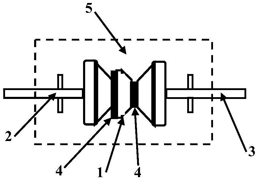
[0018] Embodiment 1: A high-efficiency processing device for a diode device, the axial diode includes a diode chip 1, a first copper lead 2, and a second copper lead 3, and one end of the first copper lead 2 is passed through a solder 4 Connected to the N pole surface of the diode chip 1, the other end of the first copper lead 2 is used as the input end of the axial type diode; one end of the second copper lead 3 is connected to the diode chip 1 through solder 4 On the P pole surface, the other end of the second copper lead 3 is used as the input end of the axial type diode, and the end of the diode chip 1, the first copper lead 2 and the second copper lead 3 in contact with the diode chip is covered by an epoxy body 5 cover;

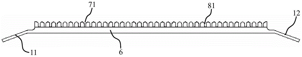
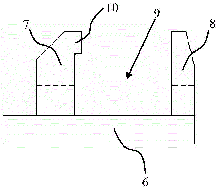
[0019] The turnover device includes a strip substrate 6, several comb teeth 7 and several orientation teeth 8, and several comb teeth 7 are located in the middle of the strip substrate 6 and arranged in a line along its length direction. The orientatio...

Embodiment 2

[0022] Embodiment 2: A high-efficiency processing device for a diode device, the axial diode includes a diode chip 1, a first copper lead 2, and a second copper lead 3, and one end of the first copper lead 2 is passed through a solder 4 Connected to the N pole surface of the diode chip 1, the other end of the first copper lead 2 is used as the input end of the axial type diode; one end of the second copper lead 3 is connected to the diode chip 1 through solder 4 On the P pole surface, the other end of the second copper lead 3 is used as the input end of the axial type diode, and the end of the diode chip 1, the first copper lead 2 and the second copper lead 3 in contact with the diode chip is covered by an epoxy body 5 cover;

[0023] The turnover device includes a strip substrate 6, several comb teeth 7 and several orientation teeth 8, and several comb teeth 7 are located in the middle of the strip substrate 6 and arranged in a line along its length direction. The orientatio...


PUM


Abstract

The invention discloses an efficient processing device for a diode device. The efficient processing device includes a bar-shaped substrate, a plurality of material combing teeth and a plurality of orientation teeth, wherein the plurality of material combing teeth are positioned at the middle of the bar-shaped substrate and straightly arranged along the length direction, the plurality of orientation teeth are positioned on one side of the bar-shaped substrate and straightly arranged along the length direction, and thereby a long slot is formed between the plurality of material combing teeth and the plurality of orientation teeth, a material combing tooth slot is formed between the two adjacent material combing teeth, a material combing tooth slot is formed between the two adjacent orientation teeth, and the spacing of the material combing tooth slots is more than the diameters of a first copper lead and a second copper lead; the material combing teeth and the orientation teeth are positioned on the same side of the bar-shaped substrate and arranged oppositely, a left handle and a right handle are respectively arranged at two ends of the bar-shaped substrate along the length direction, and the upper end of each material combing tooth is provided with a hook part stretching into the long slot. The efficient processing device can comb up the welded diode from a graphite boat and rotate for 180 degrees without dropping materials, and thereby the turnover tools is reduced, and the man efficiency and yield are improved.

Description

technical field [0001] The invention relates to the production of rectifying devices, in particular to a high-efficiency processing device for diode devices. Background technique [0002] In the prior art, in the manufacture of diodes, materials are combed onto aluminum strips through combing strips, and then the materials on the aluminum strips are transferred to the feeding rack of the forming mold. The problem brought about by this method is to increase the turnover tools, increase labor costs, and increase the risk of damage to the product caused by a process. Contents of the invention [0003] The object of the present invention is to provide a trench type Schottky semiconductor device, which improves the reliability of the device, the potential line density will be reduced at the top of the trench, and the device forward voltage drop Both the loss of the device and the device are reduced, and the leakage of the device is further reduced when the device is turned off...

Claims


Application Information

Patent Timeline
IPC IPC(8): H01L21/67
CPCH01L21/67778H01L2224/32245H01L2224/33181H01L2924/181H01L2924/00012
Inventor 韦德富蒋祖良许卫岗
Owner SUZHOU GOODARK ELECTRONICS CO LTD
Why Eureka
Try Eureka