Method for preparing optical anti-fake element
An optical anti-counterfeiting and component technology, applied in the field of optical anti-counterfeiting, can solve the problems of poor process controllability, low reliability, large error of optical anti-counterfeiting components, etc., and achieve the effect of strong process feasibility and strong process stability
- Summary
- Abstract
- Description
- Claims
- Application Information
AI Technical Summary
Problems solved by technology
Method used
Image
Examples
Embodiment Construction
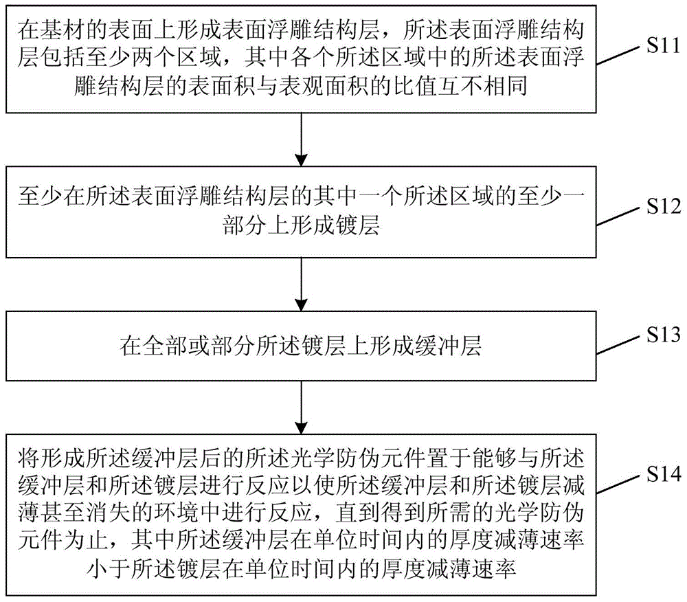
[0016] The flow chart of the method for preparing an optical anti-counterfeiting element according to the present invention will be described in detail below with reference to the accompanying drawings.
[0017] Such as figure 1 Shown, the method for preparing optical anti-counterfeiting element according to the present invention comprises the following steps:
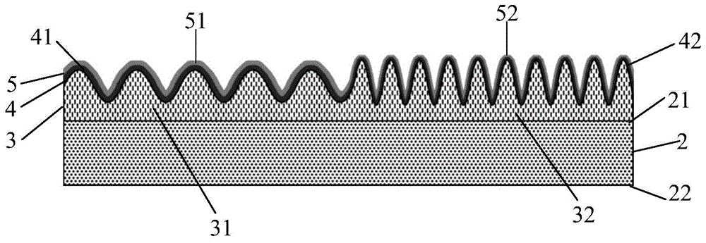
[0018] S11, forming a surface relief structure layer on the surface of the substrate, the surface relief structure layer comprising at least two regions, wherein the ratio of the surface area to the apparent area of the surface relief structure layer in each of the regions is different from each other .
[0019] Specifically, the surface relief structure layer is composed of a surface relief structure on the surface of the substrate whose height on a two-dimensional plane fluctuates and changes with position distribution. Compared with a flat surface, the surface relief structure has a larger surface area per unit ...
PUM
 Abstract
Description
Claims
Application Information

