Chip uid mapping writing method

A technology of chips and chips under test, applied in electronic circuit testing and other directions, can solve the problems of long program code, low traceability, difficult maintenance, etc., and achieve high readability, strong traceability, and easy maintenance Effect

Active Publication Date: 2018-10-16
SINO IC TECH
View PDF5 Cites 0 Cited by
  • Summary
  • Abstract
  • Description
  • Claims
  • Application Information

AI Technical Summary

Problems solved by technology

[0006] The purpose of the present invention is to provide a chip UID mapping writing method to solve the problems in the prior art that the program code is redundant, the later maintenance is difficult, and the traceability is low

Method used


Image

  • Chip uid mapping writing method

Examples


Embodiment Construction

[0021] The specific implementation manner of the present invention will be described in more detail below with reference to schematic diagrams. Advantages and features of the present invention will be apparent from the following description and claims. It should be noted that all the drawings are in a very simplified form and use imprecise scales, and are only used to facilitate and clearly assist the purpose of illustrating the embodiments of the present invention.

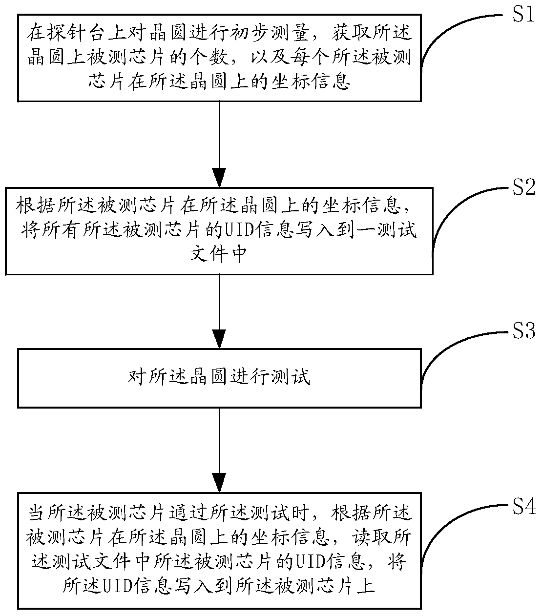
[0022] like figure 1 As shown, the present invention provides a chip UID mapping writing method, comprising the following steps:

[0023] S1: Preliminarily measure the wafer on the probe station, and acquire the number of tested chips on the wafer and the coordinate information of each tested chip on the wafer.

[0024] Specifically, there is no need to test the wafer on the probe station, it is only necessary to pre-run the wafer on the probe station to obtain the number of tested chips on the wafer, and each ...


PUM


Abstract

The invention provides a chip UID (User Identification) mapping writing-in method. The chip UID mapping writing-in method comprises the following steps: primarily measuring a wafer on a probe platform to obtain the quantity of detected chips on the wafer, and coordinate information of the detected chips on the wafer; writing UID information of the detected chips into a testing file according to the coordinate information of the detected chips on the wafer; testing the wafer; when the detected chips pass the test, reading the UID information of the detected chips in the testing file according to the coordinate information of the detected chips on the wafer; and writing the UID information into the detected chips. With the adoption of the chip UID mapping writing-in method, the conversion between a plurality of systems is avoided, codes are simple, and the readability is strong, so that the post-period maintenance is easy and the traceability is strong.

Description

technical field [0001] The invention relates to the technical field of integrated circuit testing, in particular to a chip UID mapping writing method. Background technique [0002] During the wafer test process, for some chips with special requirements, a unique UID (User Identification) number needs to be written. In the wafer test, it is the serial number of the chip, and the serial number of the chip is unique. unique, non-repetitive, and traceable. The UID information includes: serial number, batch number, chip number, coordinate information of the chip on the wafer, design company information, tape-out company information, testing company information, and time information. [0003] After the test is completed, all chips that pass the test need to be written with UID information, and then the chips that pass the packaging test in the packaging factory are finished products, and then the finished product test is performed. If the finished product test passes, the finishe...

Claims


Application Information

Patent Timeline
Patent Type & Authority Patents(China)
IPC IPC(8): G01R31/28
Inventor 顾春华凌俭波方华徐惠王锦
Owner SINO IC TECH
Why Eureka
Try Eureka