
Active silicon substrate manufacturing method

A manufacturing method and technology of silicon substrates, applied in semiconductor/solid-state device manufacturing, electrical components, circuits, etc., can solve problems such as adhesion problems, processing, and difficult problems, and achieve high moisture absorption rate, good heat dissipation, and excellent CTE matching Effect

Active Publication Date: 2017-08-04
NO 24 RES INST OF CETC
View PDF4 Cites 0 Cited by
  • Summary
  • Abstract
  • Description
  • Claims
  • Application Information

AI Technical Summary

Problems solved by technology

[0004] At present, BCB dielectric materials have been widely used in foreign countries. BCB materials are divided into two types: photosensitive and non-photosensitive. There are also researches and preliminary applications in domestic factories, but there are mainly problems of adhesion between BCB media and upper and lower materials. Other Processing Difficulties

Method used


Image

  • Active silicon substrate manufacturing method
  • Active silicon substrate manufacturing method
  • Active silicon substrate manufacturing method

Examples


Embodiment 1

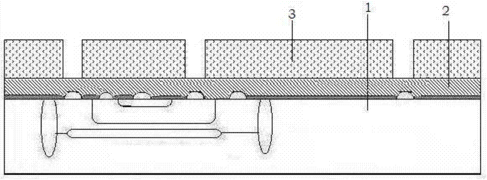
[0050] The manufacturing method of the active silicon substrate of this embodiment includes the following steps:

[0051] 1. Select Active silicon wafer 1 with a thickness of 500 microns;

[0052] 2. Fabricate the first layer of non-photosensitive BCB dielectric layer 2 on the active silicon wafer 1, specifically including:

[0053] 1) Ultrasonic cleaning of the active silicon wafer in step 1 with acetone and ethanol for 5 minutes (organic ultrasonic cleaning in this cleaning process), and then cleaning with argon plasma for 5 minutes with a cleaning power of 150W;

[0054] 2) Apply AP3000BCB tackifier, rotate at 2000 rpm for 20 minutes to dry, and then bake on a 100°C hot plate for 60 seconds;

[0055] 3) Coat the BCB solution at a coating speed of 800 rpm for 20 seconds (BCB thickness is about 5um), and bake on a 90°C hot plate for 120 seconds;

[0056] 4) Under a vacuum environment below 0.8mbar, perform soft curing on the BCB film layer. The soft curing conditions are sh...


PUM


Abstract

The invention discloses an active silicon substrate manufacturing method. The method includes the steps that firstly, a first non-photosensitive BCB medium layer is coated on and cured on an active wafer, secondly, then through holes are formed in a BCB film layer in a photoetching and etching mode, a first TiW / Au conduction band layer is manufactured on the BCB medium layer, then a second non-photosensitive BCB medium layer is coated on and cured on the first conduction band layer, then a second TiW / Au conduction layer is manufactured on the BCB medium layer, and finally a non-photosensitive BCB passivation layer and a passivation layer window are manufactured on the surface of the second TiW / Au conduction layer. By means of the active silicon substrate manufacturing method, the active chip wafer serves as circuit substrate materials, through a thin-film multilayer wiring technology, the novel BCB medium materials are adopted, a chip I / O is vertically connected with the chip level of peripheral elements, and an active silicon substrate with the high assembling efficiency and high performance and based on the active wafer is formed. The active silicon substrate manufacturing method solves the problems that a conventional 3D structure is low in assembling efficiency, large in packaged size, low in performance index and the like.

Description

technical field [0001] The invention belongs to the field of basic electrical components, and relates to a manufacturing method of a semiconductor device, in particular to a manufacturing method of an active silicon substrate. Background technique [0002] The substrate is the core component of electronic equipment, and it undertakes key functions such as mechanical support, heat dissipation and conduction. In order to meet the needs of miniaturization, multi-function and system integration of electronic products, three-dimensional (3D) system-in-package method has been paid more and more attention. There are mainly three types of 3D structures of multi-chip modules (MCMs), namely embedded 3D, active substrate 3D and stacked 3D. Among them, the active substrate has the advantages of the smallest volume, performance index, assembly density and high reliability. Therefore, the advanced system-in-package is focusing on the research of active wafer and embedded chip 3D substrat...

Claims


Application Information

Patent Timeline
Patent Type & Authority Patents(China)
IPC IPC(8): H01L21/768
CPCH01L21/76801H01L21/76877
Inventor 叶冬谢廷明罗驰杨镓溢
Owner NO 24 RES INST OF CETC
Learn More