Array type pressure measuring device based on packaging substrate

A technology of measuring device and packaging substrate, which is applied in the direction of fluid pressure measurement by changing ohmic resistance, etc., can solve the temperature state of piezoresistive sensitive strip - difficult to test characterization, difficult to predict, complex integration and assembly of multi-channel pressure test circuit system, etc. question

Pending Publication Date: 2021-06-04
明晶芯晟(成都)科技有限责任公司
View PDF0 Cites 0 Cited by
  • Summary
  • Abstract
  • Description
  • Claims
  • Application Information

AI Technical Summary

Problems solved by technology

First of all, the integration and assembly of the multi-channel pressure test circuit system is complicated, the interconnection distance between the core chip-MEMS piezoresistive sensitive chip and the subsequent processing circuit is long, and the integration degree is low. Among the representative technical solutions currently disclosed, Assemble the bare chip of the pressure gauge on the ceramic chip-PCB circuit board-metal plate stack, and gradually lead the input and output of the bare chip to the ceramic chip through wire bonding, and then to the PCB circuit board, and finally hand it over to the PCB board for assembly The amplification, digital-to-analog conversion and other modules are used for signal processing, which limits the number of pressure measurement channels per unit area, and the integration level is low
Secondly, the introduction of stress and strain during the assembly process of MEMS piezoresistive sensitive chip devices, the thermal stress caused by the difference in thermal expansion coefficient between it and other parts of the device, and the uneven temperature distribution field cause performance drift and difficult prediction, which restricts the long-term performance of the product. Stability and Overall Accuracy
Finally, in the current technical solutions, the temperature sensor in the working state of the piezoresistive sensitive chip is generally obtained through the temperature sensor assembled on the circuit board or the temperature sensor integrated on the surface of the MEMS piezoresistive sensitive chip. Because the MEMS piezoresistive sensitive chip has various thermodynamic There is self-heating in the characteristic material system and its working state, which causes the temperature state of the piezoresistive sensitive strip-test and characterization is difficult, and the temperature sensor assembled on the circuit board cannot accurately characterize the pressure of the piezoresistive sensitive chip in the working state. Sensitive to the temperature state of the strip, which limits the accuracy of temperature compensation

Method used


Image

  • Array type pressure measuring device based on packaging substrate
  • Array type pressure measuring device based on packaging substrate
  • Array type pressure measuring device based on packaging substrate

Examples


Embodiment 1

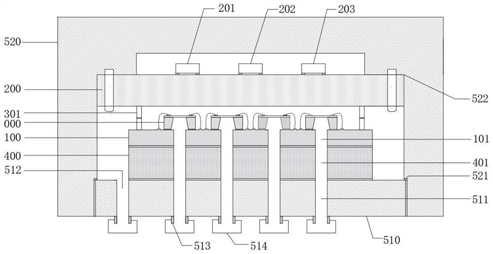
[0030] Design and integrated assembly method of array pressure measurement device based on packaging substrate such as figure 1 As shown, the pressure measurement device mainly includes a piezoresistive sensitive chip 000 , a packaging substrate 100 , a circuit board 200 , an electrical interconnection and fixing structure 300 , a gasket 400 and an alloy shell 500 .

[0031] In one embodiment of the present invention, the packaging substrate 100 is a silicon substrate or a glass substrate, further a TSV / TGV substrate.

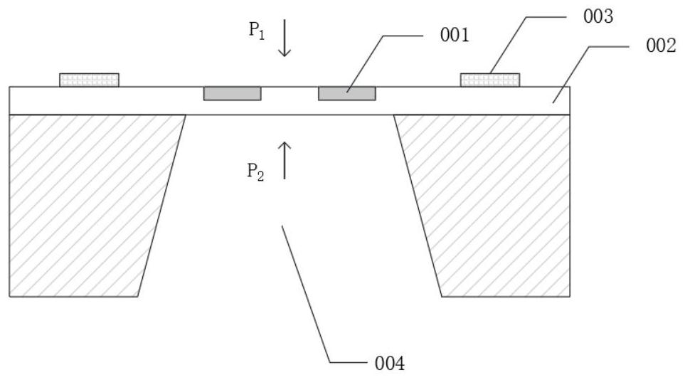
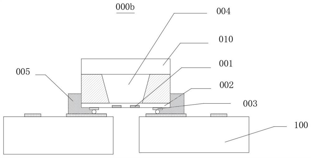
[0032] refer to figure 2 and image 3 , the piezoresistive sensitive chip 000 can be divided into a differential pressure piezoresistive sensitive chip 000a and an absolute pressure piezoresistive sensitive chip 000b. The piezoresistive sensitive chip 000 is a silicon substrate, and the piezoresistive strip 001, passivation layer 002 and Pad 003 are formed on the front of the piezoresistive sensitive chip 000 through epitaxy, oxidation, diffusion, sputtering...

Embodiment 2

[0041] refer to Figure 5 and Figure 6 The difference between this embodiment and Embodiment 1 is that the piezoresistive sensitive chip 000 is flip-chip soldered on the packaging substrate 100, and the gap between the piezoresistive sensitive chip 000 and the packaging substrate 100 is sealed with a sealing ring 005, and the sealing ring 005 can be Silicone rubber or silicone sealant is used; the packaging substrate 100 and the circuit board 200 are stacked and placed in parallel, and the two are stacked through the electrical interconnection and the fixed structure 302 to realize electrical and fixed. The height is the height of the piezoresistive sensitive chip and flip-chip welding, The electrical interconnection and fixing structure 302 can be a combination of the Pad 303 and the TSV 304 ; for the rest, refer to Embodiment 1.

Embodiment 3

[0043] refer to Figure 7 , the pressure measuring device mainly includes a piezoresistive sensitive chip 000 , a package substrate 100 , a circuit board 200 , an electrical and fixed structure 300 , a gasket 400 , an alloy shell 500 and an interconnection substrate 600 .

[0044] The difference between this embodiment and Embodiment 1 is that the front side of the piezoresistive sensitive chip 000 is welded on the interconnect substrate 600 with at least one wiring layer on the surface; integrated on the interconnect substrate 600 in the form of wire bonding or mounting; optionally, the packaged instrument amplifier circuit 601, ADC 602, MCU 603, etc. are integrated on the circuit board 200 in the form of wire bonding or mounting; The substrate 600 and the circuit board 200 are stacked and placed in parallel, and the two are stacked with the fixed structure 301 through electrical interconnection to realize electrical and fixed. The height is the height of the instrument ampli...


PUM


Abstract

The invention relates to the field of microelectronic packaging, in particular to an array type pressure measuring device based on a packaging substrate, which comprises: an alloy shell and a piezoresistive sensitive chip which is arranged in the alloy shell and is used for applying reference pressure on the front surface of the piezoresistive sensitive chip and applying external gas pressure on the back surface of the piezoresistive sensitive chip to generate pressure difference; a packaging substrate which is provided with an air guide hole, is integrated with the piezoresistive sensitive chip, and is used for providing air pressure and acting on the two surfaces of the piezoresistive sensitive chip so as to generate the pressure difference; a circuit board, wherein the circuit board and the packaging substrate are stacked and arranged in parallel, the circuit board and the packaging substrate are stacked with a fixing structure through electric interconnection, and the circuit board is used for converting the generated pressure difference into an electric signal which is in direct proportion to pressure change, outputting the electric signal and processing and calculating the electric signal; and an alloy substrate which is used for sealing the piezoresistive sensitive chip, the substrate and the circuit board in the alloy shell. According to the invention, the assembly stress can be reduced, and the internal integrated gas path system facilitates the miniaturization of the whole pressure measurement device assembly.

Description

technical field [0001] The invention relates to the field of microelectronic packaging, in particular to an array pressure measurement device based on a packaging substrate. Background technique [0002] The array multi-channel pressure measurement device is widely used in wind tunnel tests or flight tests, which can realize multi-channel rapid pressure measurement. Among them, the MEMS piezoresistive sensitive chip is the core device of the pressure measurement device, which has a decisive impact on the overall performance of the pressure measurement device. . At present, the comprehensive performance improvement of array multi-channel pressure measurement devices faces some core problems that need to be solved and optimized. First of all, the integration and assembly of the multi-channel pressure test circuit system is complicated, the interconnection distance between the core chip-MEMS piezoresistive sensitive chip and the subsequent processing circuit is long, and the i...

Claims


Application Information

Patent Timeline
Patent Type & Authority Applications(China)
IPC IPC(8): G01L9/02
CPCG01L9/02
Inventor 马盛林黄漪婧于娟练婷婷汪郅桢
Owner 明晶芯晟(成都)科技有限责任公司
Why Eureka
Try Eureka