Vertical interconnection structure for millimeter wave frequency band chip packaging
A millimeter-wave frequency band and vertical interconnection technology, which is applied in the direction of electrical components, electrical solid devices, circuits, etc., can solve the problems of poor transmission performance and achieve the effects of small signal transmission loss, easy implementation, and good isolation
- Summary
- Abstract
- Description
- Claims
- Application Information
AI Technical Summary
Problems solved by technology
Method used
Image
Examples
Embodiment 1
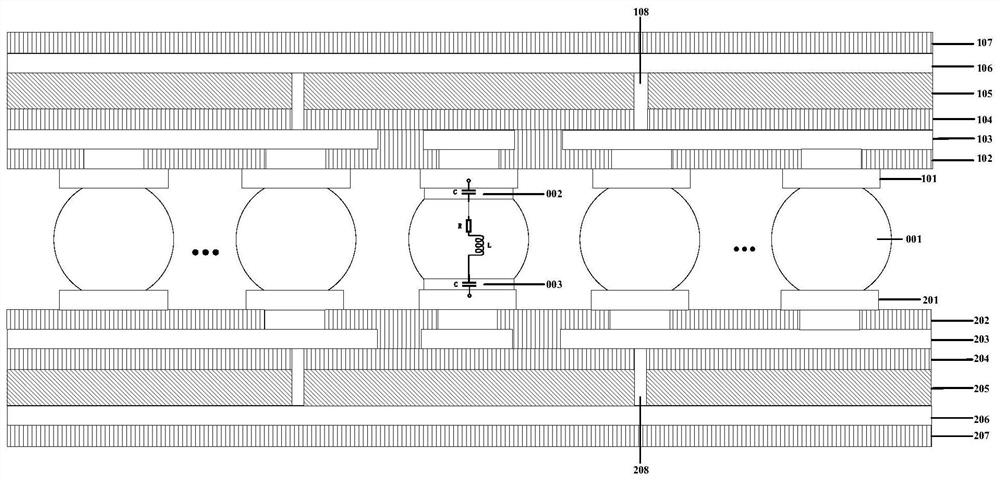
[0033] Such as figure 1 As shown, the vertical interconnection structure for chip packaging in the millimeter wave frequency band according to Embodiment 1 of the present invention respectively includes from top to bottom: a first transmission line (passivation layer 102, coplanar waveguide 103, passivation layer 104, liner Bottom 105, back conductor 106, passivation layer 107, hole 108), first metal pad 101, first dielectric 002, Bump001, second dielectric 003, second metal pad 201 and second transmission line (passivation layer 202 , coplanar waveguide 203, passivation layer 204, substrate 205, back conductor 206, passivation layer 207, hole 208).
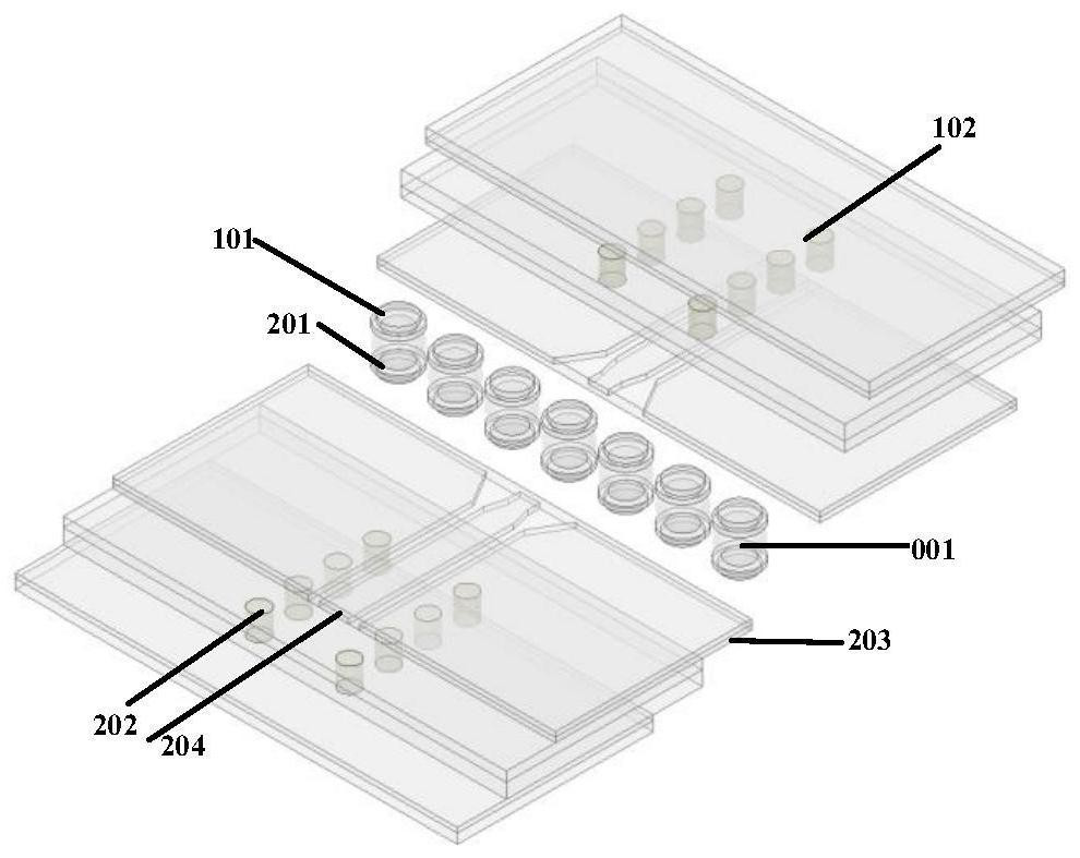
[0034] Such as figure 2 As shown, the overall structural layered diagram of the vertical interconnection structure used for millimeter-wave frequency band chip packaging in Embodiment 1 of the present invention, the structure includes: Bump001, the first metal pad 101, the second metal pad 201, and a coplanar waveguide The gro...
Embodiment 2
[0049] Such as Figure 5 As shown, the vertical interconnection structure for millimeter-wave frequency band chip packaging according to Embodiment 2 of the present invention includes: Bump001, medium 002, metal pad 101, metal pad 201, first transmission line (passivation layer 102, coplanar waveguide 103, passivation layer 104, substrate 105, backside conductor 106, passivation layer 107, hole 108), second coplanar waveguide_backside conductor_hole transmission line (passivation layer 202, coplanar waveguide 203, passivation layer 204, substrate 205, back conductor 206, passivation layer 207, hole 208), the first and second coplanar waveguide_back conductor_hole transmission line is connected together with two metal pads through Bump, wrapping dielectric around Bump001 002.
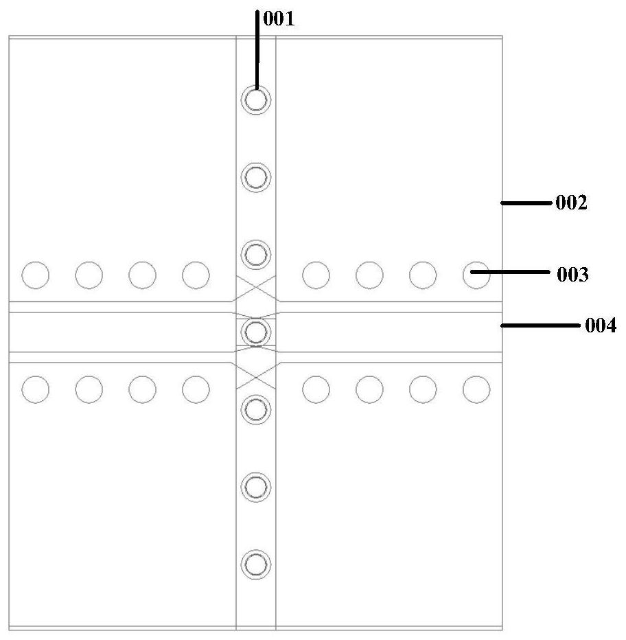
[0050] The first and second transmission lines have the same structure and size, with an impedance of 50 ohms. A passivation layer 104, 204 is designed on the top layer of the substrate 105, 205, and a ...
Embodiment 3
[0060] Such as figure 1 As shown, the vertical interconnection structure for chip packaging in the millimeter wave frequency band according to Embodiment 3 of the present invention respectively includes from top to bottom: a first transmission line (passivation layer 102, coplanar waveguide 103, passivation layer 104, liner Bottom 105, back conductor 106, passivation layer 107, hole 108), first metal pad 101, first dielectric 002, Bump001, second dielectric 003, second metal pad 201 and second transmission line (passivation layer 202 , coplanar waveguide 203, passivation layer 204, substrate 205, back conductor 206, passivation layer 207, hole 208).
[0061] The structure and size of the first transmission line and the second transmission line are the same, and the impedance is 50 ohms. Both the first transmission line and the second transmission line have a coplanar waveguide-back conductor-hole structure, and a flip-chip welding process is used to realize the connection bet...
PUM
 Abstract
Description
Claims
Application Information


