
Semiconductor device, ceramic circuit board, and semiconductor device manufacturing method

A circuit substrate and semiconductor technology, which is applied in semiconductor/solid-state device manufacturing, semiconductor devices, semiconductor/solid-state device components, etc. Problems such as bonding strength of the circuit layer

Active Publication Date: 2015-06-10
MITSUBISHI MATERIALS CORP
View PDF9 Cites 6 Cited by
  • Summary
  • Abstract
  • Description
  • Claims
  • Application Information

AI Technical Summary

Problems solved by technology

At this time, when the metal paste or oxide paste is sintered in the central part of the joint surface, the sintering of the peripheral part of the joint surface has been completed, resulting in the decomposition reaction of organic matter generated in the central part of the joint surface and the formation of metal oxide particles. The gas generated by the reduction reaction remains inside the bonding layer, and the bonding strength between the semiconductor element and the circuit layer may not be ensured
Therefore, the thermal resistance between the semiconductor element and the circuit layer increases, and the heat generated from the semiconductor element may not be efficiently transferred to the circuit layer side.

Method used


Image

  • Semiconductor device, ceramic circuit board, and semiconductor device manufacturing method
  • Semiconductor device, ceramic circuit board, and semiconductor device manufacturing method
  • Semiconductor device, ceramic circuit board, and semiconductor device manufacturing method

Examples


Embodiment

[0113] Hereinafter, the results of confirmation experiments conducted to confirm the effects of the present invention will be described.

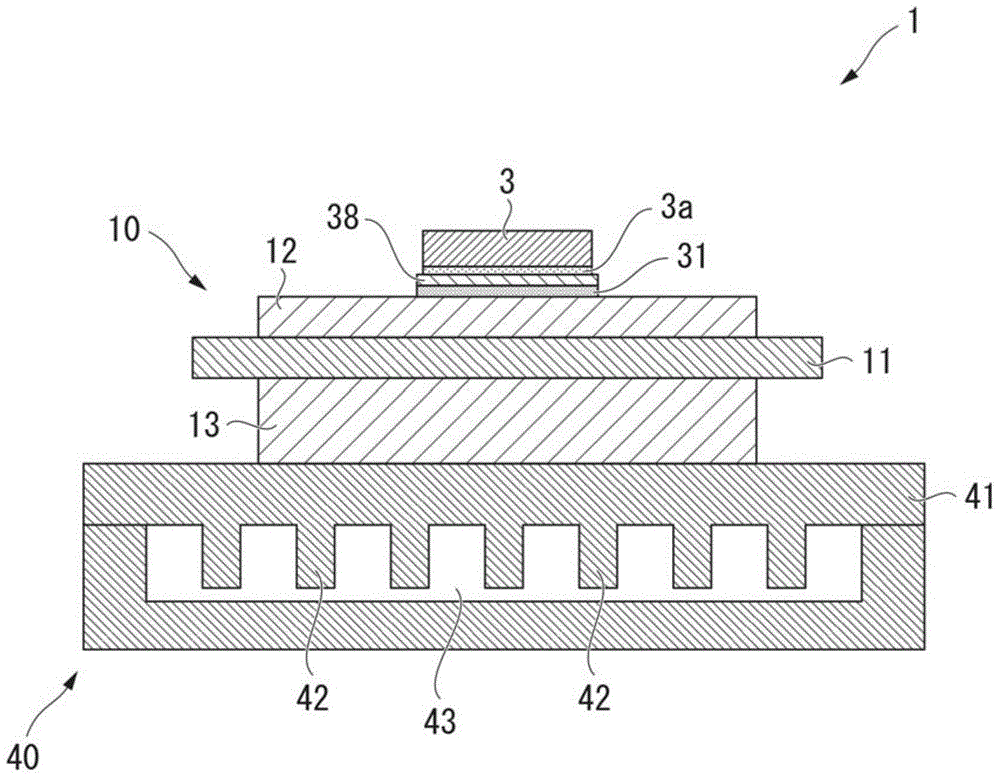
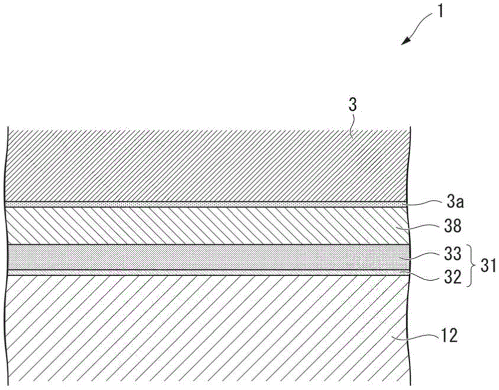
[0114] Various semiconductor devices (power modules) are produced by changing the porosity of the base layer using the ceramic circuit board shown below.

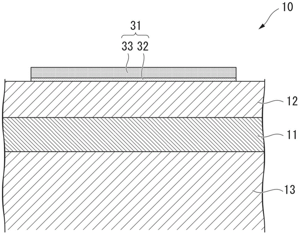
[0115] A ceramic circuit board is produced by soldering a bonded circuit layer on one side of the ceramic substrate and brazing an aluminum plate that is synthesized as a metal layer on the other side. Here, the ceramic substrate is made of AlN, and its size is 27 mm×17 mm×0.6 mm. The aluminum plate used as the circuit layer was 4N aluminum with a purity of 99.99% by mass or higher, and its size was 25 mm×15 mm×0.6 mm. The aluminum plate used as the metal layer was 4N aluminum with a purity of 99.99% or higher, and its size was 25 mm×15 mm×1.6 mm.

[0116] As the semiconductor element, a semiconductor element having a size of 13 mm×10 mm×0.25 mm was used.

[0117] Using the glass-cont...


PUM

PropertyMeasurementUnit
thicknessaaaaaaaaaa
electrical resistanceaaaaaaaaaa
viscosityaaaaaaaaaa

Abstract

A semiconductor device (1) of the present invention is provided with a circuit layer (12) formed of a conductive material, and a semiconductor element (3) mounted on the circuit layer (12). On one surface of the circuit layer (12), a base layer (31) having a porosity within a range of 5-55 % is formed, and on the base layer (31), a bonding layer (38) is formed, said bonding layer being formed of a fired body of a bonding material containing metal particles and / or metal oxide particles, and an organic material. The circuit layer (12) and the semiconductor element (3) are bonded to each other with the base layer (31) and the bonding layer (38) therebetween.

Description

technical field [0001] The present invention relates to a semiconductor device including a circuit layer made of a conductive material and a semiconductor element mounted on the circuit layer, a ceramic circuit board used in the semiconductor device, and a method of manufacturing the semiconductor device. [0002] This application claims priority based on Patent Application No. 2012-224257 for which it applied in Japan on October 09, 2012, and uses the content here. Background technique [0003] In semiconductor devices such as LEDs and power modules, semiconductor elements are bonded on a circuit layer made of a conductive material. [0004] For example, power semiconductor elements for high-power control used to control electric vehicles such as wind power generation and electric vehicles have a large amount of heat generation. Therefore, as a substrate on which the power semiconductor elements are mounted, they have been widely used, for example, on substrates made of AlN...

Claims


Application Information

Patent Timeline
Patent Type & Authority Applications(China)
IPC IPC(8): H01L21/52H01L23/36H01L25/07H01L25/18
CPCC04B37/026H01L21/52H01L23/36H01L23/3735H01L23/473H01L24/32H01L25/07H01L25/18H01L2224/73265H01L33/641H01L2924/13091H01L2924/13055H01L2924/1305H01L2924/15787C04B2237/06C04B2237/125C04B2237/126C04B2237/366C04B2237/402C04B2237/597C04B2237/708C04B2237/72H01L2924/12042H01L24/29H01L24/48H01L2224/2732H01L2224/27505H01L2224/29082H01L2224/29083H01L2224/29188H01L2224/29339H01L2224/29344H01L2224/29347H01L2224/29387H01L2224/29388H01L2224/32227H01L2224/83192H01L2224/83203H01L2924/00014H01L2924/12041H01L2224/29294H01L2224/2731H01L2224/83539H01L2224/83595H01L2224/83695H01L2224/32245H01L2224/4809H01L2224/48227H01L2224/48245H01L2924/181H01L24/83H01L2224/32225H01L2224/8384H01L2924/00H01L2924/00012H01L2924/0541H01L2924/01047H01L2224/45099H01L2224/85399H01L2224/05599H01L23/49822
Inventor 西元修司长友义幸长瀬敏之
Owner MITSUBISHI MATERIALS CORP
Learn More