CMOS on-chip direct-current negative voltage generation circuit

A technology for generating circuits and negative voltages, applied to electrical components, adjusting electrical variables, instruments, etc., can solve problems such as inability to provide DC negative voltages

Active Publication Date: 2015-06-17
NO 24 RES INST OF CETC
View PDF9 Cites 21 Cited by
  • Summary
  • Abstract
  • Description
  • Claims
  • Application Information

AI Technical Summary

Problems solved by technology

[0008] Aiming at the technical problems existing in the prior art, the present invention provides a CMOS on-chip DC negative voltage ge

Method used


Image

  • CMOS on-chip direct-current negative voltage generation circuit
  • CMOS on-chip direct-current negative voltage generation circuit
  • CMOS on-chip direct-current negative voltage generation circuit

Examples


Embodiment Construction

[0033] In order to make the technical means, creative features, goals and effects achieved by the present invention easy to understand, the present invention will be further described below in conjunction with specific illustrations.

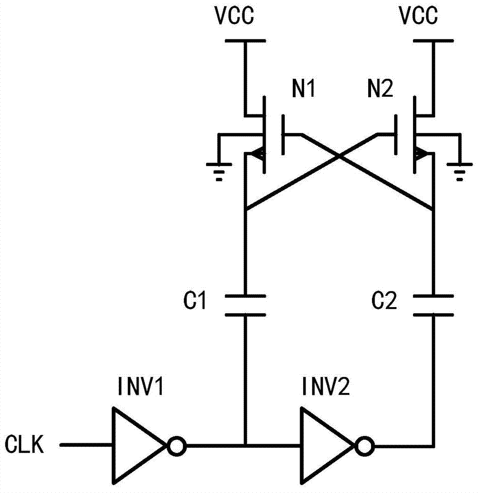
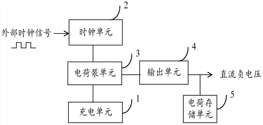
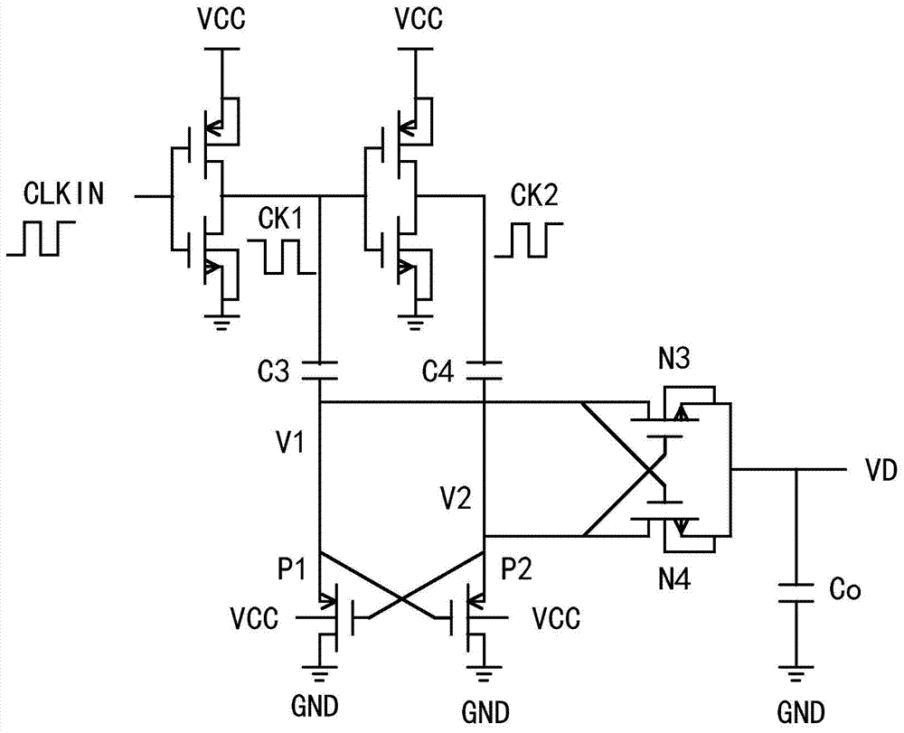
[0034] Please refer to figure 2 As shown, the present invention provides a CMOS on-chip DC negative voltage generating circuit, including a charging unit 1, a clock unit 2, a charge pump unit 3, an output unit 4 and a charge storage unit 5; wherein,

[0035] The charging unit 1 is configured to charge the charge pump unit 3;

[0036] The clock unit 2 is configured to provide the required clock signal to the charge pump unit 3;

[0037] The charge pump unit 3 is used to generate a negative pulse voltage whose amplitude is equal to the positive power supply voltage;

[0038] The output unit 4 is configured to convert the negative pulse voltage generated by the charge pump unit 3 into a DC negative voltage, the magnitude of which is equal to the...


PUM


Abstract

The invention provides a CMOS on-chip direct-current negative voltage generation circuit. The CMOS on-chip direct-current negative voltage generation circuit comprises a charging unit, a clock unit, a charge pump unit, an output unit and a charge storage unit; the charging unit is used for charging the charge pump unit, the clock unit is used for providing needed clock signals to the charge pump unit, the charge pump unit is used for generating a negative impulse voltage which is equal to a positive supply voltage in amplitude, the output unit is used for converting the negative impulse voltage generated by the charge pump unit into a direct-current negative voltage, and the direct-current negative voltage is equal to a positive supply voltage; the charge storage unit is used for storing charges brought by the charge pump unit to a negative potential, and meanwhile the direct-current negative voltage output by the output unit keeps stable in the CMOS chip working process. By means of the CMOS on-chip direct-current negative voltage generation circuit, the problem that the direct-current negative voltage is generated inside a chip under the condition that a CMOS chip single direct-current positive power source supplies power is solved.

Description

technical field [0001] The invention belongs to the field of analog / mixed signal integrated circuits, and in particular relates to a CMOS on-chip DC negative voltage generation circuit. Background technique [0002] Today's integrated circuit manufacturing process - Complementary Metal Oxide Semiconductor (CMOS) process, the substrate is a P-type semiconductor. In order to achieve effective isolation between devices, the CMOS integrated circuit chip substrate is connected to the lowest potential - ground potential, and is powered by a positive power supply voltage. [0003] As the feature size of the CMOS process develops towards deep submicron (below 90nm), the chip power supply voltage is getting lower and lower, even lower than 1V. Under such a low power supply voltage, traditional analog circuit structures (such as operational amplifiers, current sources, etc.) will not work properly. Therefore, in order to make the traditional analog circuit structure work normally un...

Claims


Application Information

Patent Timeline
IPC IPC(8): G05F1/56
CPCH03M1/54
Inventor 胡蓉彬王永禄胡刚毅陈光炳王育新付东兵张正平朱璨
Owner NO 24 RES INST OF CETC
Why Eureka
Try Eureka