
Device substrate

A component substrate and substrate technology, applied in the direction of instruments, electrical digital data processing, data processing input/output process, etc., can solve the problems of large impedance value, low touch sensitivity of touch panel, etc., and achieve the effect of good conductivity

Inactive Publication Date: 2015-06-24
WINTEK CORP
View PDF4 Cites 14 Cited by
  • Summary
  • Abstract
  • Description
  • Claims
  • Application Information

AI Technical Summary

Problems solved by technology

However, indium tin oxide has the disadvantage of relatively large impedance value, so it may cause the situation that the touch sensitivity of the touch panel is not high

Method used


Image

  • Device substrate
  • Device substrate
  • Device substrate

Examples


Embodiment Construction

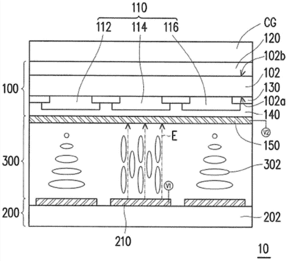
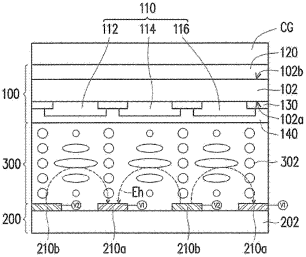
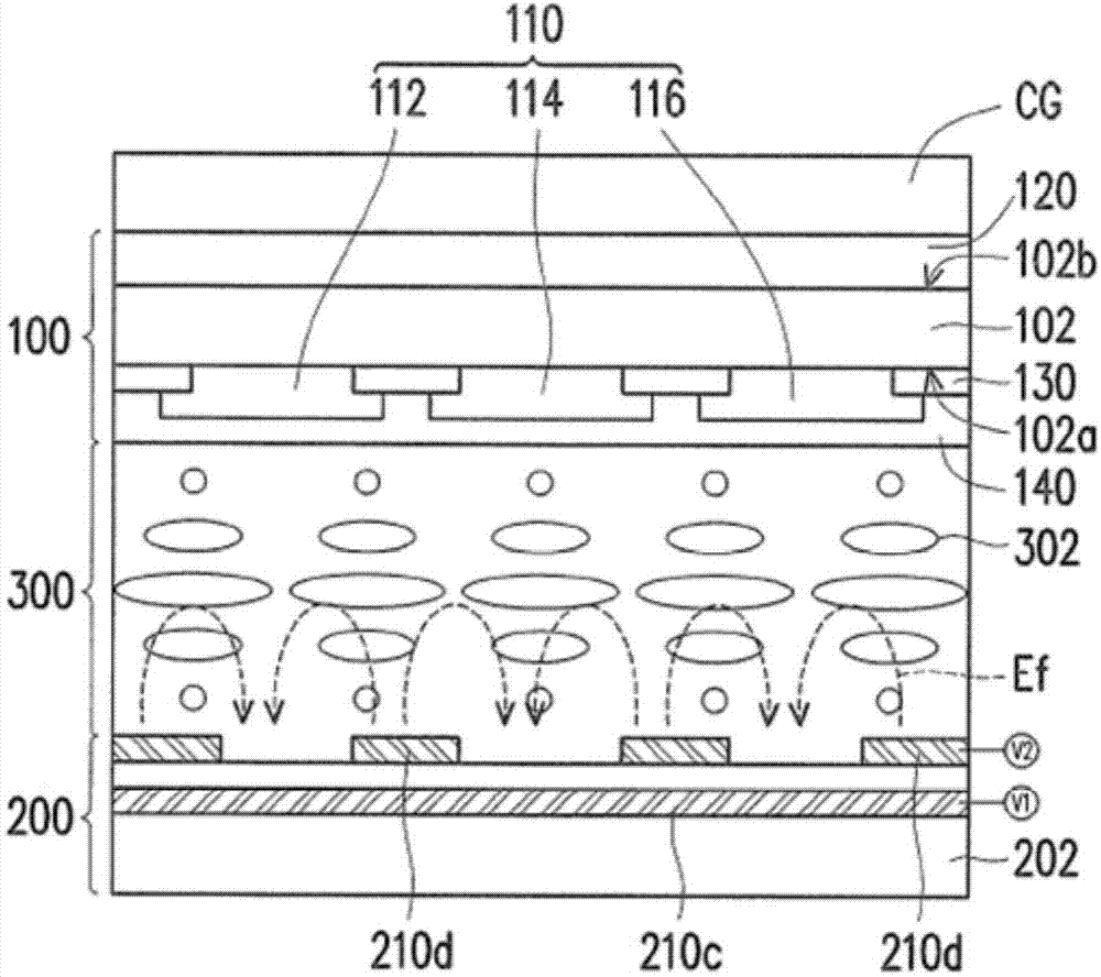
[0162] Figure 1A It is a schematic cross-sectional view of a touch display panel according to an embodiment of the invention. Please refer to Figure 1A The touch display panel 10 includes an element substrate 100, a counter substrate 200, and a display medium layer 300. The counter substrate 200 and the element substrate 100 are disposed oppositely, and the display medium layer 300 is located on the element substrate 100 and the counter substrate. Between 200.

[0163] The device substrate 100 includes a first substrate 102, a color filter layer 110, a conductive member 120, a black matrix layer 130, an insulating layer 140, and a common electrode layer 150. The first substrate 102 may be a color filter substrate, which has a first side 102a and a second side 102b opposite to the first side 102a, wherein the second side 102b is a side close to the user's touch operation. The conductor member 120 is located between the second side 102b and a cover plate CG, wherein an adhesive la...


PUM


Abstract

A device substrate including a substrate and a conductor element is provided. The substrate has a first side and a second side opposite to each other. The conductor element is disposed on the second side, and at least one portion of the conductor element is composed of a conductor mesh layer.

Description

Technical field [0001] The present invention relates to a device substrate, and more particularly to a device substrate with a conductor grid layer. Background technique [0002] Generally speaking, capacitive touch panels can generally include two types: added-on type and in / on-cell type. The externally attached capacitive touch panel usually first manufactures the touch components on a substrate to form a touch panel, and then attaches the touch panel to the outer surface of the display. Therefore, the externally attached touch The control panel will have a certain thickness. In addition, a common integrated touch panel directly integrates the touch component on the element substrate of the display, which is very beneficial to the thinning and weight reduction of the display. [0003] In the manufacturing process of the integrated touch panel, a transparent conductive material such as indium tin oxide (ITO) is usually used as the material of the touch electrode. In this way, a...

Claims


Application Information

Patent Timeline
Patent Type & Authority Applications(China)
IPC IPC(8): G06F3/044
Inventor 王文俊李崇维许景富许辰合
Owner WINTEK CORP
Learn More