Fin-type field effect transistor forming method

A fin-type field effect and transistor technology, which is applied in semiconductor devices, semiconductor/solid-state device manufacturing, electrical components, etc., to achieve high deposition quality

Inactive Publication Date: 2015-06-24
SEMICON MFG INT (SHANGHAI) CORP
View PDF4 Cites 18 Cited by
  • Summary
  • Abstract
  • Description
  • Claims
  • Application Information

AI Technical Summary

Problems solved by technology

[0005] The performance of the fin field effect transistor needs to be further improved

Method used


Image

  • Fin-type field effect transistor forming method
  • Fin-type field effect transistor forming method
  • Fin-type field effect transistor forming method

Examples


Embodiment Construction

[0034] As mentioned in the background art, the performance of the fin field effect transistor formed in the prior art needs to be further improved.

[0035] Research has found that performing ion implantation on the source and drain regions of the fin field effect transistor to form the source and drain tends to cause more defects in the source and drain regions, and because the fin The size of the fins of the fin field effect transistors is smaller, which is more likely to affect the performance of the formed fin field effect transistors.

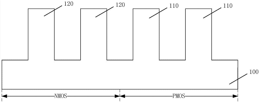
[0036] The source and drain electrodes formed on the fin portion of the fin field effect transistor by using the in-situ doping process can reduce the damage caused by ion implantation to the fin portion, but due to the gradual shrinking of the fin field effect transistor size, adjacent The distance between the fins of the N-type Fin Field Effect Transistor and the P-Type Fin Field Effect Transistor is small, and the distance between the e...


PUM


Abstract

The invention discloses a fin-type field effect transistor forming method. The forming method comprises steps: a semiconductor substrate is provided, wherein the semiconductor substrate is provided with an NMOS region and a PMOS region, a first fin part is formed on the PMOS region, and a second fin part is formed on the NMOS region; a first dielectric layer is formed on the semiconductor substrate; a gate structure crossing the first fin part and the second fin part is formed on the surface of the first dielectric layer; a mobile chemical vapor deposition process is adopted to form a second dielectric layer on the first dielectric layer; a part of the second dielectric layer at the top part of the first fin part at two sides of the gate structure is removed to enable the top surface of the first fin part to be exposed; a first semiconductor layer is formed on the surface of the first fin part; an oxide layer is formed on the surface of the second semiconductor layer; a part of the second dielectric layer at the top part of the second fin part at two sides of the gate structure is removed to enable the top surface of the second fin part to be exposed; and a second semiconductor layer is formed on the surface of the second fin part.

Description

technical field [0001] The invention relates to the technical field of semiconductors, in particular to a method for forming a fin field effect transistor. Background technique [0002] With the continuous development of semiconductor process technology, the process node is gradually reduced, and the gate-last (gate-last) process has been widely used to obtain an ideal threshold voltage and improve device performance. However, when the feature size of the device is further reduced, even if the gate-last process is adopted, the structure of the conventional MOS field effect transistor can no longer meet the requirements for device performance. Fin field effect transistor (Fin FET) is obtained as a multi-gate device. received widespread attention. [0003] Fin field effect transistor is a common multi-gate device, figure 1 A schematic diagram of a three-dimensional structure of a fin field effect transistor in the prior art is shown. [0004] like figure 1 As shown, it inc...

Claims


Application Information

Patent Timeline
Patent Type & Authority Applications(China)
IPC IPC(8): H01L21/336H01L21/8238
CPCH01L29/785H01L21/8238H01L21/823821H01L29/66795
Inventor 三重野文健
Owner SEMICON MFG INT (SHANGHAI) CORP
Why Eureka
Try Eureka