Organic image sensor and method of forming the same

An image sensor, organic technology, applied in the field of image sensors, can solve the problems of organic image sensors to be further improved, limiting incident light absorption, etc.

Active Publication Date: 2017-11-03
SEMICON MFG INT (SHANGHAI) CORP
View PDF5 Cites 0 Cited by
  • Summary
  • Abstract
  • Description
  • Claims
  • Application Information

AI Technical Summary

Problems solved by technology

[0005] 2. The structure and design of the traditional sensor limit the absorption of incident light, while the organic image sensor can absorb all the light reaching the sensor, which makes its photosensitivity 1.2 times higher than that of the traditional sensor, even in low light. get a clean screen
[0006] 3. The silicon photodiode in the silicon-based CMOS image sensor has a minimum thickness of 3 microns, which limits its incident light angle to only 30-40 degrees
[0007] However, the performance of existing organic image sensors still needs to be further improved

Method used


Image

  • Organic image sensor and method of forming the same
  • Organic image sensor and method of forming the same
  • Organic image sensor and method of forming the same

Examples


Embodiment Construction

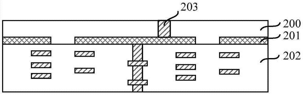
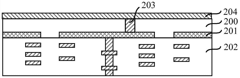
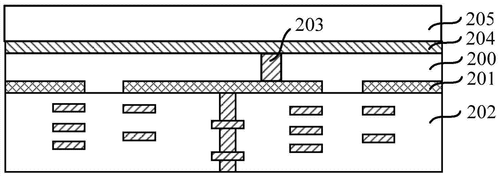
[0035] After research, the structure of the existing organic image sensor includes: a substrate, several discrete pixel lower electrodes on the substrate; an organic photoelectric conversion layer on the pixel lower electrode; and an upper electrode on the organic photoelectric conversion layer. When external light is incident from above the upper electrode, the organic photoelectric conversion layer induces light to generate charges, and receives the induced charges through the upper electrode and the corresponding pixel lower electrode. However, since the existing organic photoelectric conversion layer has a whole-layer structure, interference between adjacent pixel units is likely to occur during light sensing. Light is also irradiated into the organic photoelectric conversion layer corresponding to the adjacent pixel unit, thereby forming a dark current in the adjacent pixel unit.

[0036] To this end, the present invention provides an organic image sensor and a method for...


PUM


Abstract

An organic image sensor and a method for forming the same, wherein the organic image sensor includes: a semiconductor substrate, the semiconductor substrate includes a first surface and a second surface opposite to the first surface, the first surface of the semiconductor substrate A pixel circuit is formed on the surface, and a plurality of pixel lower electrodes arranged in a matrix are formed on the second surface of the semiconductor substrate, and the pixel lower electrode is connected to the pixel circuit through a through-hole interconnection structure in the semiconductor substrate; Several discrete organic photoelectric conversion layers on the second surface of the semiconductor substrate, each organic photoelectric conversion layer covers the corresponding pixel lower electrode, and there is an isolation layer between adjacent organic photoelectric conversion layers and between adjacent pixel lower electrodes ; An upper electrode located on the organic photoelectric conversion layer. The interference between adjacent pixel units of the organic image sensor of the present invention is small, and the generation of dark current is prevented.

Description

technical field [0001] The present invention relates to the field of image sensors, in particular to an organic image sensor and a method for forming the same. Background technique [0002] Image sensors have been widely used in cameras, medical devices, cellular phones, automobiles, and other applications. A more common image sensor is a silicon-based CMOS (complementary metal-oxide-semiconductor) image sensor (CIS). Each pixel of a silicon-based image sensor typically contains a photosensitive element such as a photodiode and one or more transistors for reading signals from the photosensitive element. However, with the continuous innovation of technology, the continuous progress of society and the continuous improvement of sensor performance, the existing silicon-based CMOS sensors cannot meet the existing application needs. Therefore, the industry proposes a new type of sensor-organic image sensor. Sensor (organic photoconductive image sensor). [0003] Organic image s...

Claims


Application Information

Patent Timeline
Patent Type & Authority Patents(China)
IPC IPC(8): H01L27/30
Inventor 三重野文健肖德元洪中山
Owner SEMICON MFG INT (SHANGHAI) CORP
Why Eureka
Try Eureka