

Field programmable logic array and serial data receiving and converting method
A technology of programming logic and analog-to-digital converters, which is applied in the direction of electrical digital data processing, input/output process of data processing, instruments, etc., can solve the problem that the time offset between the latch clock and the data channel cannot be dynamically compensated, and achieve dynamic Compensate time offset and realize the effect of dynamic compensation
- Summary
- Abstract
- Description
- Claims
- Application Information
AI Technical Summary
Problems solved by technology
Method used
Image

Examples
Embodiment Construction
[0046] The following will clearly and completely describe the technical solutions in the embodiments of the present invention with reference to the accompanying drawings in the embodiments of the present invention. Obviously, the described embodiments are only some, not all, embodiments of the present invention. Based on the embodiments of the present invention, all other embodiments obtained by persons of ordinary skill in the art without making creative efforts belong to the protection scope of the present invention.
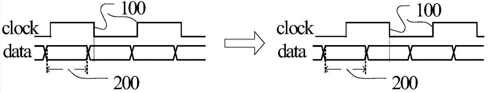
[0047] The invention provides a field programmable logic array to solve the problem in the prior art that the phase-locked loop resources of the field programmable logic array cannot be fully used and at the same time dynamically compensate the time offset from the latch clock to the data channel.
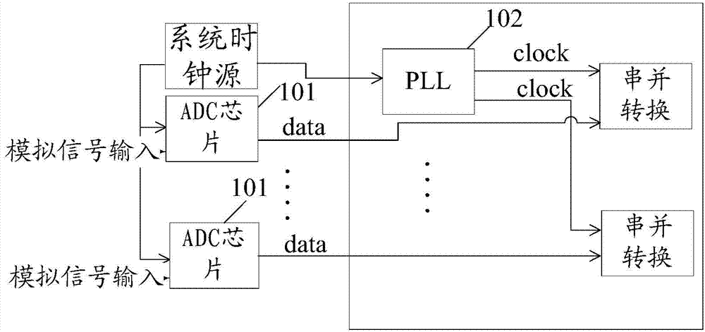
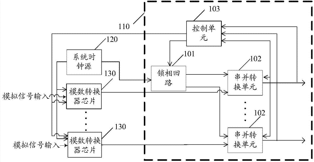
[0048] Specifically, such as image 3 As shown, the field programmable logic array 110 is connected to the system clock source 120 and N analog-to-digital converte...
PUM
 Abstract
Description
Claims
Application Information