
Electronic device

A technology for electronic components and components, which is applied to printed circuit components, electrical components, components of fixed capacitors, etc., and can solve problems such as sound and sound

Active Publication Date: 2015-07-01
TDK CORP
View PDF8 Cites 23 Cited by
  • Summary
  • Abstract
  • Description
  • Claims
  • Application Information

AI Technical Summary

Problems solved by technology

Recently, when electronic components using such external terminals are mounted on a circuit board, there is a problem that a phenomenon such as sound occurs.

Method used


Image

  • Electronic device
  • Electronic device
  • Electronic device

Examples


no. 1 Embodiment approach

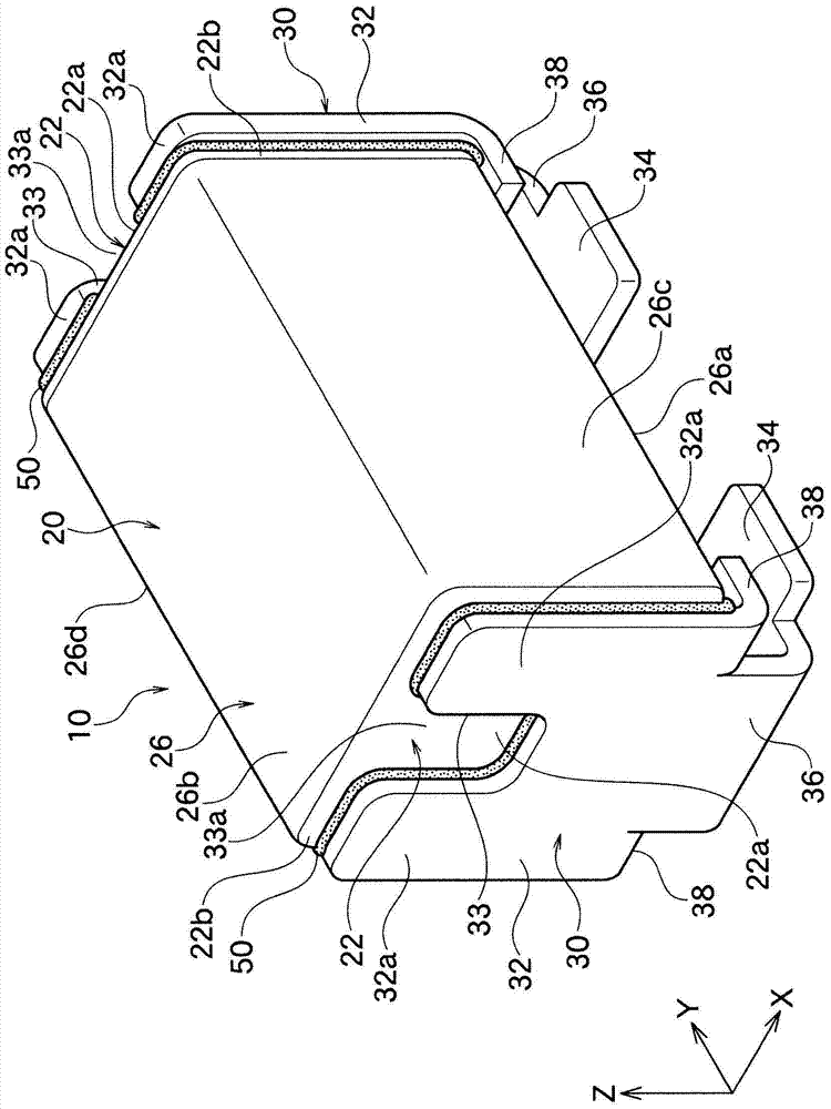
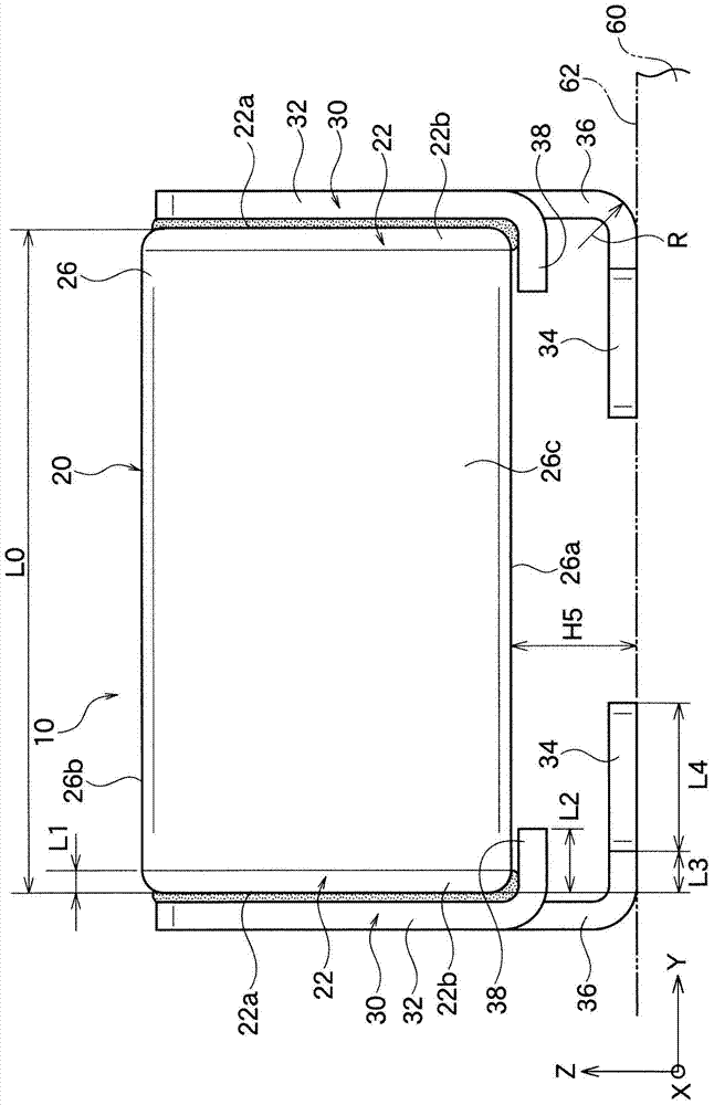
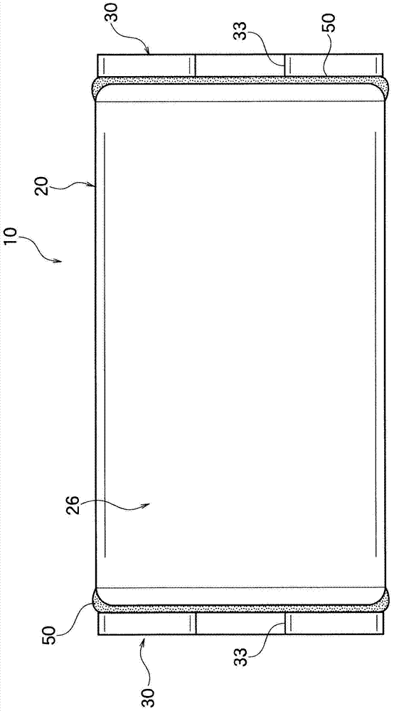
[0062] figure 1 It is a schematic perspective view showing a ceramic capacitor 10 as an electronic component according to the first embodiment of the present invention. The ceramic capacitor 10 has a chip capacitor 20 as a chip component, and a pair of metal terminals (external terminals) 30 respectively attached to both end faces of the chip capacitor 20 in the Y-axis direction.

[0063] In addition, in the description of each embodiment, the ceramic capacitor in which the pair of metal terminals 30 is mounted on the chip capacitor 20 has been described as an example, but the ceramic electronic component of the present invention is not limited to this, and may be other than Electronic components having metal terminals 30 are mounted on chip components other than capacitors.

[0064] The chip capacitor 20 has a capacitor body 26 and a pair of terminal electrodes 22 respectively formed on both end faces of the capacitor body 26 in the Y-axis direction. The capacitor element b...

no. 2 Embodiment approach

[0100] Figure 12 It is a perspective view of a ceramic capacitor 10A according to a second embodiment of the present invention. The ceramic capacitor 10A according to this embodiment is not Figure 1 to Figure 11 The ceramic capacitor 10 according to the first embodiment shown has the same structure as those described below, and exhibits the same functions and effects. Therefore, the common parts are given the same reference numerals and the common parts are omitted. instruction of.

[0101] Such as Figure 12 As shown, in this embodiment, the terminal electrode connecting portion 32A of the terminal electrode 30A is not formed. figure 1 Groove 33 is shown. Ceramic capacitor 10A of this embodiment is not formed figure 1 Other than the grooves 33 shown, the same functions and effects as those of the ceramic capacitor 10 of the first embodiment are exerted.

no. 3 Embodiment approach

[0103] Figure 13 It is a perspective view of a ceramic capacitor 10B according to the third embodiment of the present invention. The ceramic capacitor 10B according to this embodiment except Figure 1 to Figure 11 The ceramic capacitor 10 according to the first embodiment shown has the same structure as those described below, and exhibits the same functions and effects. Therefore, the common parts are given the same reference numerals and the common parts are omitted. instruction of.

[0104] Such as Figure 13 As shown, in this embodiment, the length in the Y-axis direction of the side electrode portion 22b of the terminal electrode 22 formed on the end surface of the element body 26 of the chip capacitor 20B is longer than that of the side electrode portion 22b of the terminal electrode 22 in the first embodiment. The length in the Y-axis direction is longer. The ceramic capacitor 10B of this embodiment has the same function as that of the first embodiment except that t...


PUM


Abstract

An external terminal 30 comprises a terminal electrode connection part 32 connected to the terminal electrode 22 to face to the end surface of the element body 26; a mounting connection part 34 connectable to a mounting surface 62; and a joint part 36 which joins the terminal electrode connection part 32 with the mounting connection part 34 to separate one side surface 26a of the element body 26 closest to the mounting surface 64 therefrom. A width W1 of the joint part 36 along a direction parallel to the mounting surface 62 is smaller then a width W0 of the terminal electrode connection part 32.

Description

technical field [0001] The present invention relates to electronic components connected to external terminals, for example, composed of metal terminals. Background technique [0002] As electronic components such as ceramic capacitors, in addition to ordinary chip components that are directly mounted on a board or the like by a single body, electronic components in which external terminals such as metal terminals are mounted on chip components have been proposed. Electronic components equipped with external terminals have been reported to relieve the deformation stress received by the chip components from the substrate after mounting, or to protect the chip components from impact, etc., and have been obtained in fields requiring durability and reliability. used. [0003] In an electronic component using an external terminal, one end of the external terminal is connected to a terminal electrode of a chip component, and the other end is connected to a mounting surface such as...

Claims


Application Information

Patent Timeline
Patent Type & Authority Applications(China)
IPC IPC(8): H01G4/30H01G4/232
CPCH01G4/012H01G4/30H01G4/01H01G4/12H01G4/248H01G4/008H01G2/02H01G2/06H01G4/232H05K1/0271
Inventor 前田信小林一三增田淳黑嶋敏浩
Owner TDK CORP
Learn More