Film-like light shielding plate and stop, light amount adjusting stop device or shutter using the film-like light shielding plate
A thin-film, light-shielding plate technology, applied in the direction of aperture, shutter, optics, etc., can solve the problem of not being able to obtain light-shielding properties, and achieve the effect of light weight and excellent adhesion
- Summary
- Abstract
- Description
- Claims
- Application Information
AI Technical Summary
Problems solved by technology
Method used
Image
Examples
Embodiment 1~5, comparative example 1~3
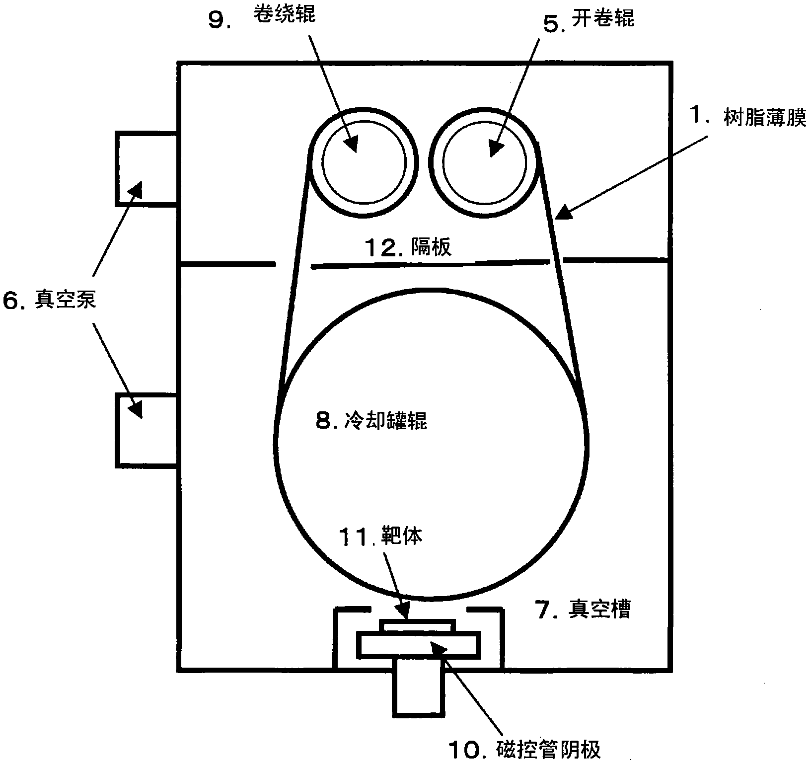
[0133] Using a polyimide (PI) film with a film surface roughness (Ra) of 0.05 μm and a thickness of 25 μm, a film with a predetermined film thickness is formed on a non-heated substrate through the aforementioned film formation procedure. Titanium oxide carbide films with the same film thickness and the same composition were formed on both sides of the film by the same manufacturing method. The temperature of the substrate surface at the time of film formation was measured with a thermal label (manufactured by NOF Giken Kogyo Co., Ltd.) attached to the film substrate and a reflection thermometer. The substrate surface temperature during film formation was all 80 to 85°C.
[0134] Table 1 shows the results of forming a titanium oxide film on a polyimide (PI) film substrate to produce a film-shaped light-shielding plate. In the table, the composition of the sintered target body used for the production of the film and the film forming conditions, the composition of the obtained ...
Embodiment 6, comparative example 4
[0145] In addition to changing the total film thickness of the titanium carbide oxide film formed on the surface of the film to 360nm (180nm on each side) (Example 6) and to 240nm (120nm on each side) (Comparative Example 4), the same process as in Example 1 was carried out. The same method is used to manufacture film-shaped visors. The results are shown in Table 1.
[0146] As indicated by the surface resistance values in the table, all indicate electrical conductivity. Thereby, the problem of dust adsorption due to electrostatic charging is less likely to occur.
[0147] From the X-ray diffraction measurement of the films of Example 6 and Comparative Example 4, it was found that films with excellent crystallinity could be obtained in the same manner as in Example 1.
[0148] The film-shaped light-shielding plate of Comparative Example 4 produced by forming a titanium carbide oxide film with a total film thickness of 240 nm had an average optical density of less than 4.0 ...
Embodiment 7, comparative example 5
[0150] In addition to changing the total film thickness of the titanium carbide oxide film formed on the surface of the film to 500nm (250nm on each side) (Example 7) and to 220nm (110nm on each side) (Comparative Example 5), the same process as in Example 3 was carried out. The same method is used to manufacture a film-shaped visor. The results are shown in Table 1.
[0151] The surface resistance values shown in the table all represent conductivity. This makes it difficult to generate static electricity and cause a problem of dust adsorption.
[0152] From the X-ray diffraction measurement of the films of Example 7 and Comparative Example 5, it can be seen that a film having excellent crystallinity can be obtained in the same manner as in Example 1.
[0153] The film-shaped light-shielding plate of Comparative Example 5 produced by forming a titanium carbide oxide film with a total film thickness of 220 nm had an average optical density of 3.68 at a wavelength of 400 to ...
PUM
 Abstract
Description
Claims
Application Information


