Metallic carbide/adamantine (MeC/DLC) nanometer multi-layer film material and method for preparing the same
A metal carbide and nano-multilayer technology, which is applied in the direction of metal material coating process, coating, layered products, etc., can solve the problems of large internal stress, insufficient smooth and delicate surface of the film layer, fast deposition rate, etc., and achieve improved Interface binding force, energy controllable range, and the effect of improving micro-roughness
- Summary
- Abstract
- Description
- Claims
- Application Information
AI Technical Summary
Problems solved by technology
Method used
Image
Examples
Embodiment 1
[0020] Double Ti targets are used, and the gas is high-purity Ar and N 2 and CH 4 , the substrate is Cr12MoV die steel.
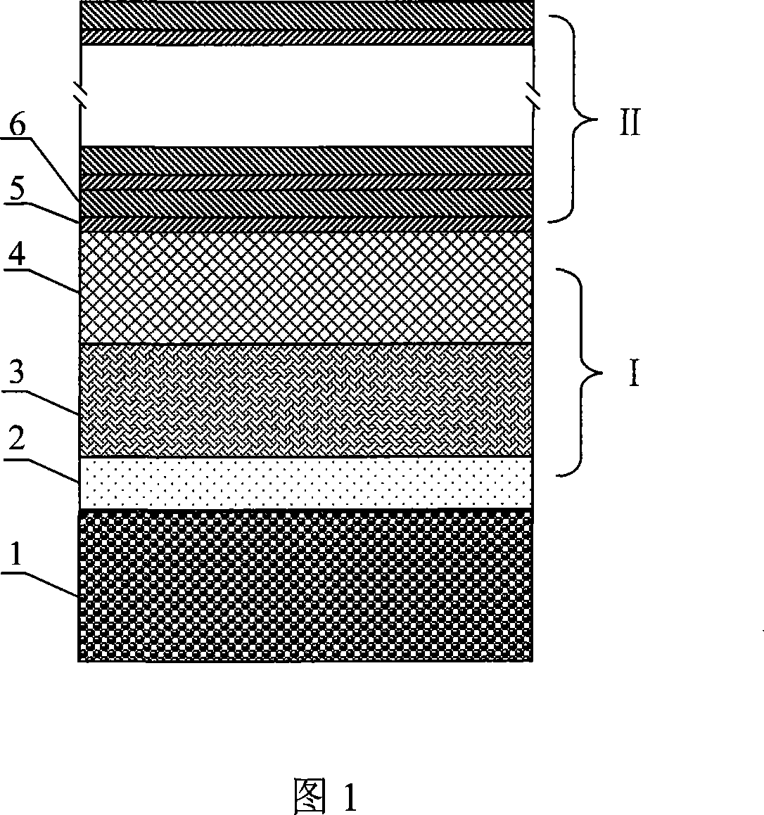
[0021] Operate sequentially according to the technological process and parameters listed in Table 1. The thicknesses of the transition layer Ti / TiN / TiCN deposited by magnetron sputtering were 0.2, 0.4, and 0.3 μm, respectively; the thickness of the TiC monolayer film deposited by magnetron sputtering and ion beam alternately was 1 nm, and the thickness of the DLC monolayer film was 3 nm. The film thickness of the layer was 3.0 μm. The total thickness of the film layer is 3.9 μm, the hardness value is HV2500, the film / substrate bonding force is 60N, and the friction coefficient of the film layer is 0.12.
[0022] Table 1 Embodiment 1 specific process flow table
[0023]
Embodiment 2
[0025] Double Cr targets are used, and the gas is high-purity Ar and N 2 and C 2 h 2 , the base material is Ti6Al4V titanium alloy.
[0026] Operate sequentially according to the technological process and parameters listed in Table 2. The transition layer Cr / CrN / CrCN was deposited by magnetron sputtering, with a thickness of 0.1, 0.3, and 0.3 μm respectively; the multilayer CrC / DLC was deposited alternately by magnetron sputtering and ion beam, and the thickness of deposited CrC single layer was 1nm, DLC The thickness of the monolayer film is 2 nm, and the thickness of the multilayer film is 2.4 μm. The total thickness of the film layer is 3.1 μm, the hardness value is HV2700, the film / substrate bonding force is 80N, and the friction coefficient of the film layer is 0.1.
[0027] Table 2 Embodiment 2 specific process flow table
[0028]
Embodiment 3
[0030] Cr and W targets are used, and the gas is high-purity Ar and N 2 and C 2 h 2 , the substrate is YT5 cemented carbide.
[0031] Operate sequentially according to the technological process and parameters listed in Table 3. The transition layer Cr / CrN / CrCN was deposited by magnetron sputtering, with a thickness of 0.2, 0.3, and 0.3 μm, respectively; the multilayer film WC / DLC was deposited alternately by magnetron sputtering and ion beam, and the thickness of the deposited WC single layer was 1.5nm. DLC monolayer film thickness is 3nm, multilayer film thickness is 2.7μm. The total thickness of the film layer is 3.5 μm, the hardness value is HV4300, the film / substrate bonding force is 65N, and the friction coefficient of the film layer is 0.12.
[0032] Table 3 Embodiment 3 specific technological process table
[0033]
PUM
| Property | Measurement | Unit |
|---|---|---|
| Thickness | aaaaa | aaaaa |
| Thickness | aaaaa | aaaaa |
| Thickness | aaaaa | aaaaa |
Abstract
Description
Claims
Application Information
