
How the transistor is formed

A transistor, dry etching technology, applied in semiconductor devices, semiconductor/solid-state device manufacturing, electrical components, etc., can solve problems such as the large difference in the depth of the Σ-shaped groove and the large difference in the depth of the rectangular groove 06. The effect of enhancing controllability

Active Publication Date: 2017-12-29
SEMICON MFG INT (SHANGHAI) CORP
View PDF4 Cites 0 Cited by
  • Summary
  • Abstract
  • Description
  • Claims
  • Application Information

AI Technical Summary

Problems solved by technology

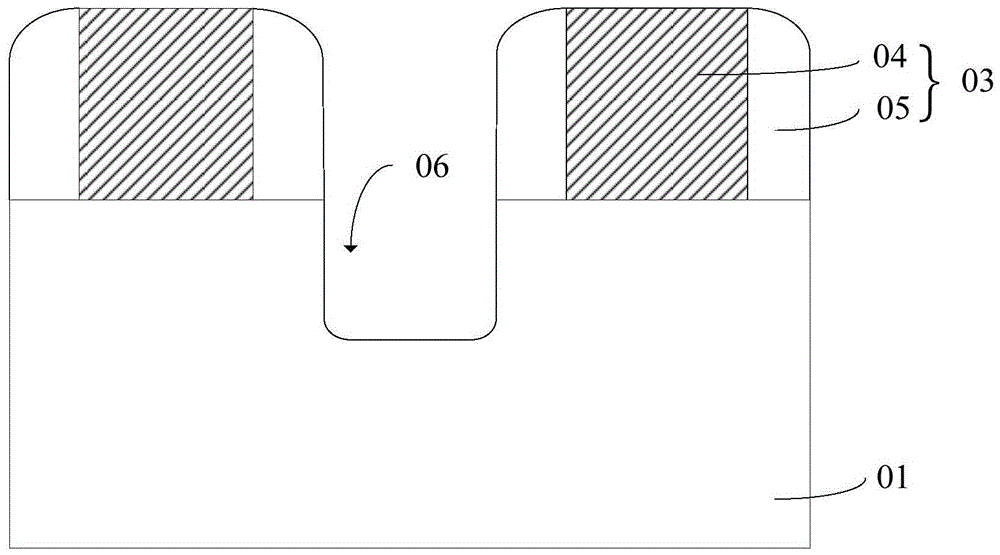
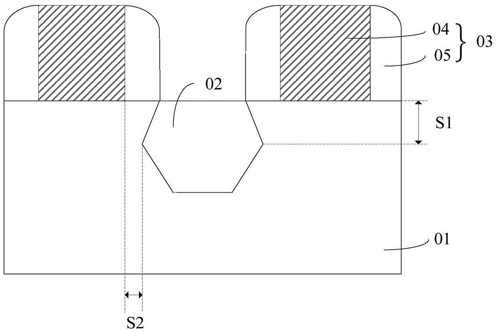
In addition, in the process of forming rectangular grooves 06 by dry etching in the prior art, the depths of rectangular grooves 06 of different sizes are quite different, and the depths of rectangular grooves 06 of the same size located in the central area and the edge area of ​​the wafer are also different. , so that the depth of the Σ-shaped grooves formed by wet etching of different rectangular grooves 06 is also quite different

Method used


Image

  • How the transistor is formed
  • How the transistor is formed
  • How the transistor is formed

Examples


Embodiment Construction

[0038] In the process of forming Σ-shaped grooves in the prior art, how to better control dry etching to form grooves with a uniform depth and reduce the vertical and lateral distances of the Σ-shaped grooves has become an urgent problem to be solved.

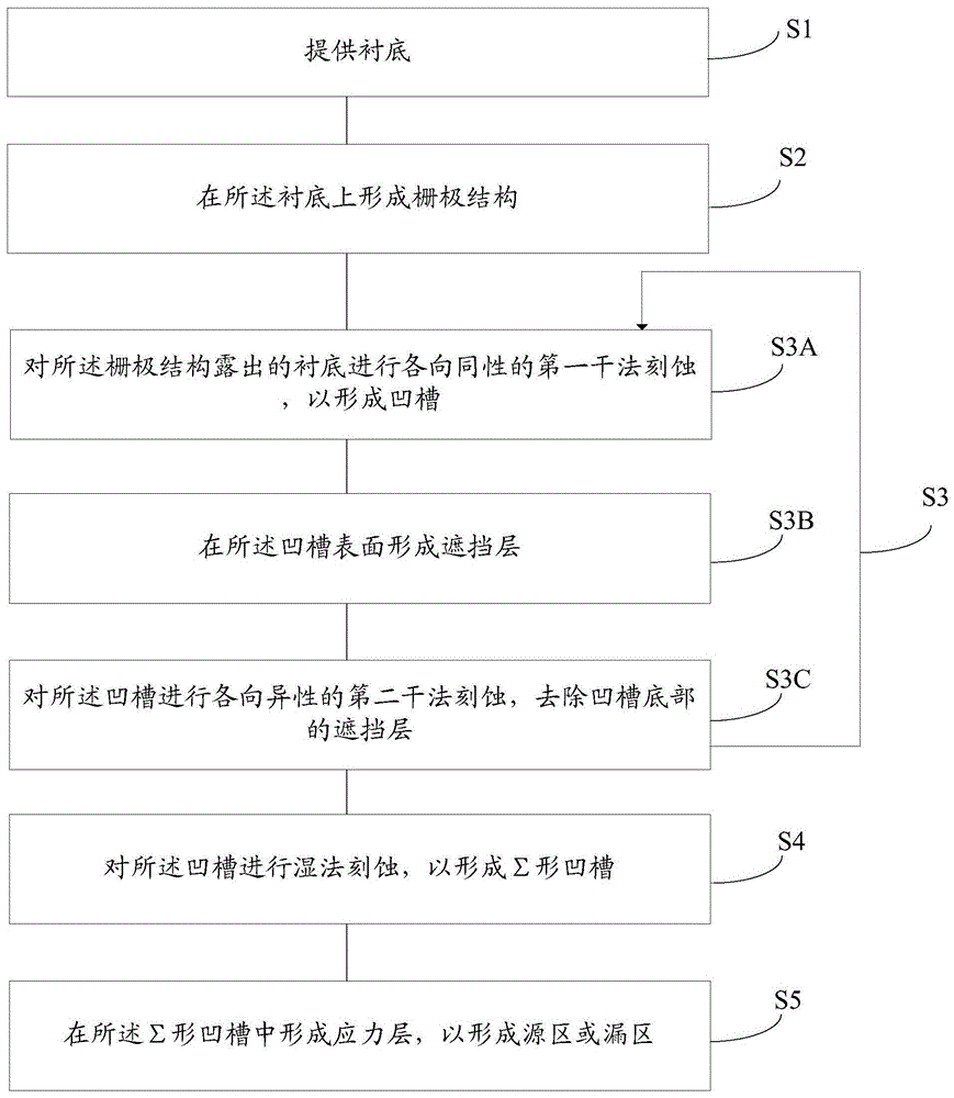
[0039] In order to solve the above technical problems, the present invention provides a method for forming a transistor, which can form an altar-shaped groove with a concave side wall in the substrate, and wet-etch the altar-shaped groove to form a Σ-shaped groove The vertical distance and the lateral distance of the groove are smaller, and the stress layer is formed in the Σ-shaped groove to form the source region or the drain region, which can optimize the performance of the transistor. And the etching of the groove is divided into repeated steps of multi-step isotropic and anisotropic dry etching, which enhances the controllability of dry etching, so that grooves of different sizes may be located in the center of the wafer T...


PUM


Abstract

The invention provides a forming method of a transistor, wherein a source region and a drain region are formed by employing a stress technology, a groove is formed by dry etching a substrate, and a capitalized sigma-shaped groove is formed by wet etching the groove. When forming the groove by the dry etching, the process of forming the groove comprises multiple times of substrate processing. The substrate processing comprises the following steps performed sequentially: performing an isotropic first dry etching to the exposed substrate of a grid electrode structure, so as to form the groove; covering a silicon oxide layer on the surface of the groove; and performing an anisotropic second dry etching to the groove. Accordingly, the shape of the groove formed thereby is approximate to a jar having a flat bottom. The capitalized sigma-shaped groove formed by wet etching the groove in the shape of the jar is uniform in depth and short in both the vertical distance as well as the horizontal distance, thus the performance of the source region and the drain region of the stress layer formed inside the capitalized sigma-shaped groove can be increased.

Description

technical field [0001] The invention relates to the field of semiconductors, in particular to a method for forming a transistor. Background technique [0002] In existing semiconductor devices, stress technology can improve the carrier mobility of the channel region in the semiconductor device. By providing tensile stress or compressive stress to the channel region, the effect of improving the carrier mobility of CMOS devices is achieved. Thereby improving the performance of the transistor. [0003] For example: form a Σ-shaped groove in the substrate corresponding to the source region and the drain region of the PMOS transistor, then epitaxially grow a silicon-germanium layer in the Σ-shaped groove, and perform ion implantation on the silicon-germanium layer to form the source region and the drain region, the silicon germanium layer can apply compressive stress to the channel of the PMOS transistor. [0004] refer to figure 1 , figure 2 , showing a cross-sectional view...

Claims


Application Information

Patent Timeline
Patent Type & Authority Patents(China)
IPC IPC(8): H01L21/336H01L21/3065
CPCH01L21/30655H01L29/66477H01L29/7848
Inventor 王新鹏陈勇
Owner SEMICON MFG INT (SHANGHAI) CORP
Learn More