Eureka AIR delivers breakthrough ideas for toughest innovation challenges, trusted by R&D personnel around the world.

Micro blind hole manufacturing method for flexible packaging substrate

A flexible packaging and manufacturing method technology, which is applied in semiconductor/solid-state device manufacturing, electrical components, circuits, etc., can solve problems such as surface copper and black hole layer faults, difficult cleaning of carbon powder, difficulty of hole filling and electroplating, etc., to achieve easy fill effect

Active Publication Date: 2015-07-01
AKM ELECTRONICS TECH SUZHOU
View PDF4 Cites 6 Cited by
  • Summary
  • Abstract
  • Description
  • Claims
  • Application Information

AI Technical Summary

Problems solved by technology

[0002] The wiring of flexible packaging substrates is getting denser and denser, especially some BGA pads are getting smaller and smaller, and the required size of via holes is also getting smaller and smaller; currently, blind via holes below 50um have been developed. Under normal circumstances, the thickness of PI is still maintained at 25um or 50um. The micro-blind hole with an aperture ratio greater than 1:1 is behind the black hole. It is difficult for the micro-etching liquid to penetrate into the bottom of the hole, which makes it difficult to clean the carbon powder. Blind hole micro-etching lines are cleaned multiple times, and cleaning will cause faults between the surface copper and the black hole layer, which will cause great difficulty in hole filling plating

Method used


Image

  • Micro blind hole manufacturing method for flexible packaging substrate
  • Micro blind hole manufacturing method for flexible packaging substrate
  • Micro blind hole manufacturing method for flexible packaging substrate

Examples


Embodiment Construction

[0025] The present invention will be further described below in conjunction with accompanying drawing.

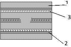
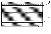
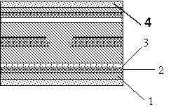
[0026] In the figure: copper foil layer 1, polyimide layer 2, adhesive layer 3, dry film 4, carbon powder layer 5.

[0027] as attached figure 1 As shown, the present invention uses a 12um thick buried blind hole four-layer board as the base material, and the middle connecting layer can be a polyimide layer 2 of 25 or 50um, a polyester layer or a polyethylene naphthalate layer, The connection layer is covered with a copper foil layer 1, and the connection layer is covered on the base material through an adhesive layer 3;

[0028] as attached figure 2 As shown, the 12um-thick buried blind hole four-layer board substrate is subjected to copper reduction treatment, so that the surface copper thickness is reduced from 12um to about 4um;

[0029] as attached image 3 As shown, a dry film 4 is attached to the surface of the thinned four-layer substrate with blind holes for p...


PUM

PropertyMeasurementUnit
Thicknessaaaaaaaaaa

Abstract

The invention discloses a micro blind hole manufacturing method for a flexible packaging substrate, and belongs to the ultrathin FPC manufacture technology; the manufacturing method comprises the following steps: step 1, pasting a protection on the single side or the surface of a multi-layer plate; step 2, laser drilling; step 3, plasma degumming; step 4, black hole; step 5, etching outside the line; 6, removing copper surface protection layer; step 7, pore-filling and electroplating; the micro blind hole manufacturing method for the flexible packaging substrate can reduce copper thickness of the surface copper, the copper surface is protected before drilling the blind hole, the micro etching ring is formed without influence of micro etching for having fault layer phenomenon to the black hole layer.

Description

technical field [0001] The invention discloses a method for manufacturing blind micro-holes on a flexible packaging substrate, which belongs to the ultra-thin FPC manufacturing process. Background technique [0002] The wiring of flexible packaging substrates is getting denser and denser, especially some BGA pads are getting smaller and smaller, and the required size of via holes is also getting smaller and smaller; currently, blind via holes below 50um have been developed. Under normal circumstances, the thickness of PI is still maintained at 25um or 50um. The micro-blind hole with an aperture ratio greater than 1:1 is behind the black hole. It is difficult for the micro-etching liquid to penetrate into the bottom of the hole, which makes it difficult to clean the carbon powder. The micro-etched line of the blind hole has been cleaned many times, and the cleaning will cause faults between the surface copper and the black hole layer, which will cause great difficulty in h...

Claims


Application Information

Patent Timeline
IPC IPC(8): H01L21/48
CPCH01L21/4878
Inventor 刘燕
Owner AKM ELECTRONICS TECH SUZHOU
Why Eureka
Eureka Blog
Learn More