Method for preserving scanning electron microscope (SEM) sample

A preservation method and scanning electron microscope technology, which can be used in the manufacture of circuits, electrical components, semiconductor/solid-state devices, etc., can solve the problems of high cost, isolation, copper oxidation, etc., and achieve the effect of low cost, lower cost, and improved success rate.

Active Publication Date: 2015-07-08
SHANGHAI HUALI MICROELECTRONICS CORP
View PDF4 Cites 1 Cited by
  • Summary
  • Abstract
  • Description
  • Claims
  • Application Information

AI Technical Summary

Problems solved by technology

However, if the copper metal layer of the sample has been exposed, it is very easy to oxidize in the air (such as Figure 4 shown)
To solve this problem, the samples are usually stored in a nitrogen cabinet or a vacuum cabinet, but this solution requires the purchase of professional equipment, which is expensive, and because it cannot be completely isolated from the air when placed in a nitrogen cabinet or a vacuum cabinet, sometimes it will Copper Oxidation Problems Occur
In addition, during the storage of all types of SEM samples, the surface of the SEM sample may also be damaged by some accidental contact, such as tweezers.

Method used


Image

  • Method for preserving scanning electron microscope (SEM) sample
  • Method for preserving scanning electron microscope (SEM) sample
  • Method for preserving scanning electron microscope (SEM) sample

Examples


Embodiment Construction

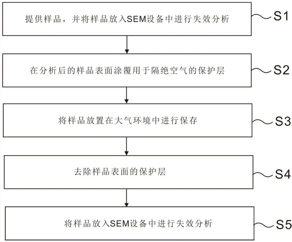
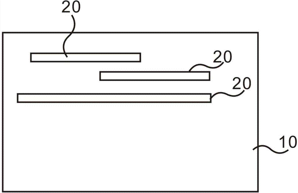
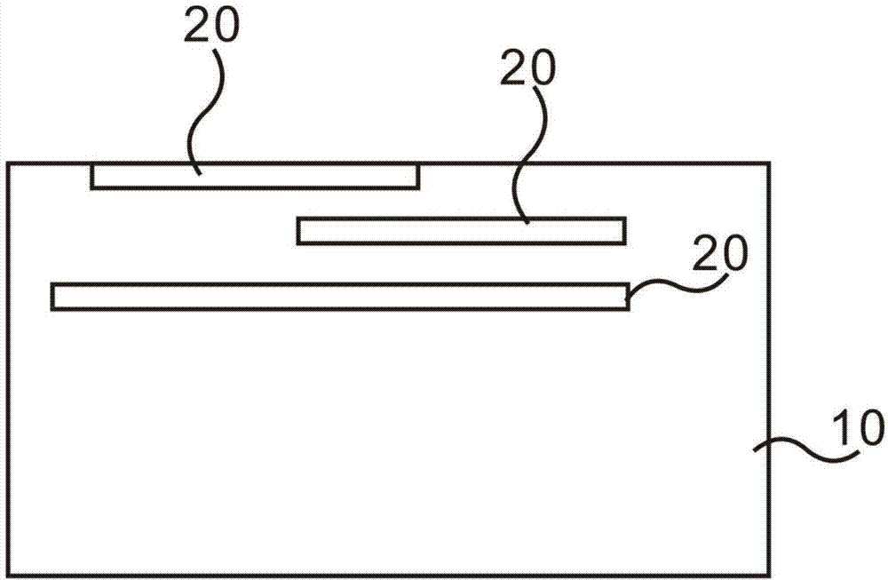
[0023] In order to make the content of the present invention clearer and easier to understand, the content of the present invention will be further described below in conjunction with the accompanying drawings. Of course, the present invention is not limited to this specific embodiment, and general replacements known to those skilled in the art are also covered within the protection scope of the present invention. Secondly, the present invention is described in detail by means of schematic diagrams. When describing the examples of the present invention in detail, for the convenience of explanation, the schematic diagrams are not partially enlarged according to the general scale, which should not be used as a limitation of the present invention.

[0024] The above and other technical features and beneficial effects will be combined with the embodiments and the accompanying Figure 1 to Figure 6 The storage method of the scanning electron microscope sample of the present inventi...


PUM


Abstract

The invention relates to the technical field of semiconductor technologies, and provides a method for preserving a scanning electron microscope (SEM) sample. The method includes the steps that the sample is provided first, the sample is placed into SEM equipment to be subjected to failure analysis, then the surface of the analyzed sample is coated with a protective layer used for isolating air, afterwards, the sample is placed in the atmospheric environment to be preserved, when the sample needs to be subjected to failure analysis again, the protective layer on the surface of the sample is eliminated, and finally the sample is placed into the SEM equipment to be subjected to failure analysis. The method for preserving the SEM sample is reliable, easy to implement and low in cost, the problem that the surface of the SEM sample is likely to be damaged or oxidized in the failure analysis process in the prior art is solved, the success rate of failure analysis can be improved by technicians in the field through the method, and the failure analysis cost is lowered.

Description

technical field [0001] The invention relates to the technical field of semiconductor manufacturing, in particular to a method for storing samples of a scanning electron microscope. Background technique [0002] Integrated Circuits (Integrated Circuit, IC) follow the evolution of Moore's Law, the integration level is continuously improved, and the feature size is continuously reduced. In the ever-shrinking device structure, the defects that cause device failure are getting smaller and smaller. Although various defects in most manufacturing processes can be caught by defect detection systems, it is impossible to tell the producer why these defects occur. Scanning Electron Microscope (SEM) is the most commonly used failure analysis equipment. SEM can be used to observe the sample cross section or surface in a subtle way. The magnification of SEM can range from thousands of times to hundreds of thousands of times, and the resolution can reach 3nm, so it can meet the needs of m...

Claims


Application Information

Patent Timeline
Patent Type & Authority Applications(China)
IPC IPC(8): H01L21/66H01L21/02
CPCH01L21/02H01L22/34
Inventor 陈强
Owner SHANGHAI HUALI MICROELECTRONICS CORP
Why Eureka
Try Eureka