GaN power device drain electrode modulation circuit
A power device and drain modulation technology, applied in the direction of power amplifiers, etc., can solve the problem of modulation device gate-source voltage limiting power device discharge circuit design, modulation device driving ability, etc., to achieve rapid discharge, logic control safety, and circuit design simple effect
- Summary
- Abstract
- Description
- Claims
- Application Information
AI Technical Summary
Problems solved by technology
Method used
Image
Examples
Embodiment Construction
[0017] The technical solution of the present invention will be further elaborated below in conjunction with the accompanying drawings.
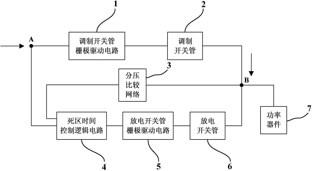
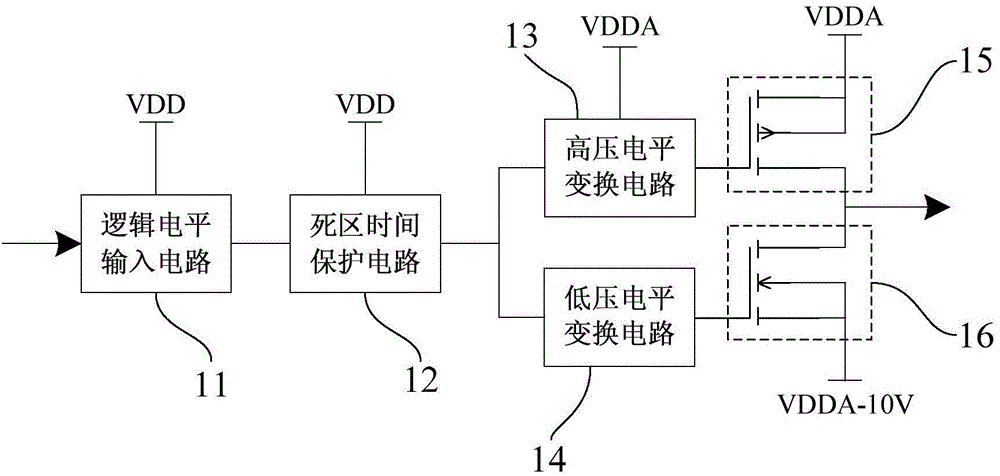
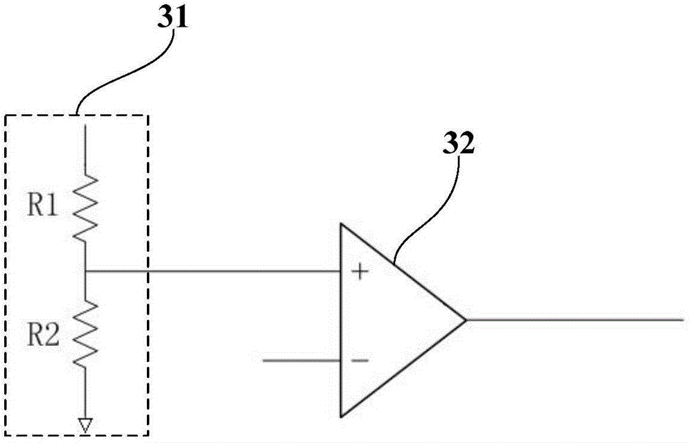
[0018] The total circuit block diagram of the present invention is as figure 1 As shown, it includes a modulation switch tube gate drive circuit 1, a modulation switch tube 2, a voltage divider comparison network 3, a dead time control logic circuit 4, a discharge switch tube gate drive circuit 5, a discharge switch tube 6 and a power device 7. The modulated input signal is from one end of the modulated switching tube gate drive circuit 1 ( figure 1 middle point A) input, the modulated drive signal is formed after the grid drive circuit 1 of the modulated switch tube and sent to the gate of the modulated switch tube 2, the drain of the modulated switch tube 2 is connected to one end of the power device 7, the discharge switch tube 6 The drain and the input terminal of the voltage divider comparison network 3 are connected ( figure 1 at poin...
PUM
 Abstract
Description
Claims
Application Information


