
Apparatus and method for manufacturing micro-nano structure

A technology of micro-nano structure and manufacturing method, which is applied in the direction of micro-structure devices, manufacturing micro-structure devices, micro-structure technology, etc., can solve problems such as tip discharge, high jet voltage threshold, Taylor cone enlargement, etc., and achieve electric field distribution Concentration, small induced voltage threshold, green and simple process

Inactive Publication Date: 2017-06-16
GUANGDONG UNIV OF TECH
View PDF6 Cites 0 Cited by
  • Summary
  • Abstract
  • Description
  • Claims
  • Application Information

AI Technical Summary

Problems solved by technology

[0005] 1. An additional high-voltage electric field is required, which has a certain risk in the working environment, and because the near-field spinning uses a high-voltage electric field, when the distance between the direct writing nozzle and the substrate is close, it is easy to produce tip discharge phenomenon, and when the distance is long, it is easy to produce instability such as jet whipping Phenomenon, which makes it difficult for precise patterned direct writing of micro-nano structures;
[0006] 2. Traditional near-field electrospinning direct writing often uses a capillary as the direct writing nozzle, which is easy to clog, and the electric field strength distribution between the nozzle and the collecting substrate is uneven, which affects the precise and stable deposition positioning of the jet;
However, the voltage threshold for forming a jet is relatively high, and it is difficult to accurately match the optimal relationship between the voltage value, liquid supply flow rate, jet flow rate, and substrate movement speed. When the relationship does not match, it is easy to cause the Taylor cone to become larger and unstable. , thus causing difficulties in the precise positioning and deposition of the jet; and the jet is easily disturbed by various factors during the movement process, and is prone to instability; moreover, due to the influence of inertia, gravity and other factors, it is difficult to achieve rapid and effective start and stop of the jet , causing difficulties for industrial applications;
[0008] 4. Traditional near-field electrospinning direct writing is only suitable for single nozzle direct writing, and the efficiency is low. When using multi-nozzle direct writing, the electric field interference between nozzles is serious. How to realize multi-nozzle jet deposition positioning control and high-precision patterns Transformation remains a challenge
[0009] Due to the inherent technical limitations of the near-field electrospinning direct writing technology, it is difficult to achieve high-precision and array patterning of the mask

Method used


Image

  • Apparatus and method for manufacturing micro-nano structure

Examples


Embodiment 1

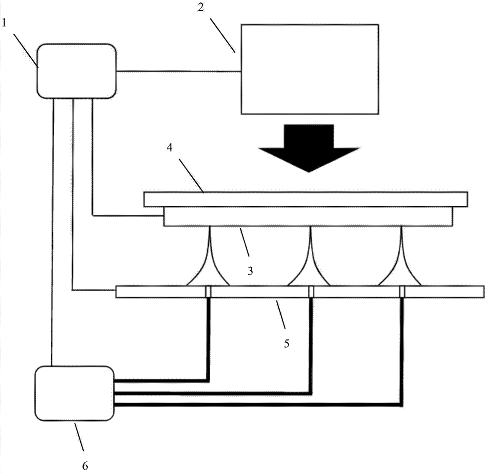
[0067] 1) Utilize computer-aided design software to design the two-dimensional micro-nano geometric figure structure of the required mask, and then convert the figure structure into outline data and filling data;

[0068] 2) Fill poly(lactic-co-glycolic acid, PLGA) into the infusion device, and the supply speed of the liquid material can be controlled by the control system;

[0069] 3) The infusion device has multiple outputs, which can be controlled by the control system to achieve selective output;

[0070] 4) Under the radiation of the heating source, LiNbO 3 The crystal generates an induced electric field, so that the PLGA rheologically stretches under the action of the thermally induced electric field to form a Taylor cone, and the tip of the Taylor cone contacts the receiving substrate;

[0071] 5) The radiation intensity of the heating source is controlled by the control system, and the speed of extensional rheology is controlled;

[0072] 6) Adopt CNC X, Y, Z axis pr...


PUM

PropertyMeasurementUnit
thicknessaaaaaaaaaa
thicknessaaaaaaaaaa

Abstract

The invention discloses a micro-nano structure manufacturing device and method. The device includes a control system, a heat supply source, a receiving substrate, a thermoelectric material, an extruding substrate, and an infusion device. The manufacturing method of the micro-nano structure, the steps are: 1) converting the graphic structure into contour data and filling data; 2) under the action of an induced electric field, the flow dynamic polymer material rheologically stretches to form a Taylor cone; 3) realizes masking Fabrication of the film; 4) Forming the coating; 5) Forming grooves with the desired geometric structure on the coating; 6) Realizing the etching of the substrate; 7) Removing the coating. The manufacturing method of the micro-nano structure of the present invention can avoid the related shortcomings of the traditional near-field electrospinning direct writing technology. The manufacturing method of the micro-nano structure of the present invention does not involve a chemical corrosion process, and the process is green and simple with low cost.

Description

technical field [0001] The invention relates to a micro-nano structure manufacturing device and method. Background technique [0002] The generation of micro-nanostructures or patterns is the most critical step in the fabrication of microelectronics and micro-nano-electromechanical systems (MEMS / NEMS). In the process of microelectronics manufacturing and grating manufacturing, photolithography technology is the most complex, core and expensive technology in the manufacturing process, and the manufacture of masks is extremely critical. This process transfers the designed geometry on the mask plate to the photoresist through photochemical reaction, exposure and development, and prepares for the later etching of the substrate material. The function of the mask plate is to selectively block light, electron beams, X-rays, etc., so as to realize graphic transfer, so the geometry of the mask plate fundamentally determines the quality of the finished product. At present, the geome...

Claims


Application Information

Patent Timeline
Patent Type & Authority Patents(China)
IPC IPC(8): B81C1/00
Inventor 房飞宇陈新王晗陈新度刘强吕元俊李克天
Owner GUANGDONG UNIV OF TECH
Learn More