
Touch control panel, touch control module and laminating method therefor

A touch module and touch panel technology, applied in the direction of instruments, electrical digital data processing, data processing input/output process, etc., can solve the impact of expanding the accuracy of touch panel detection, poor optical effect, distance and medium Changes in electrical coefficients, etc.

Inactive Publication Date: 2015-07-29
ELAN MICROELECTRONICS CORPORATION
View PDF3 Cites 3 Cited by
  • Summary
  • Abstract
  • Description
  • Claims
  • Application Information

AI Technical Summary

Problems solved by technology

As mentioned above, when the touch panel 80 is touched and deflected, the distance d between it and the liquid crystal panel 70 changes immediately, even because the distance between the two is very small, when the touch panel 80 is deformed, it is easy will touch the liquid crystal panel 70, that is, when the touch panel 80 deforms, it is likely to cause changes in distance and dielectric coefficient at the same time.
In this situation, the detection accuracy of the touch panel 80 is naturally significantly affected.
[0013] It can be seen from the above that the bonding of word-of-mouth glue has the advantages of simple technology and low cost, but the word-of-mouth glue forms an air gap between the touch panel and the liquid crystal panel, so the optical effect is poor, and once the touch panel is deformed under pressure, It will cause a relatively large change in equivalent capacitance, and expand the impact on the correctness of touch panel detection

Method used


Image

  • Touch control panel, touch control module and laminating method therefor
  • Touch control panel, touch control module and laminating method therefor
  • Touch control panel, touch control module and laminating method therefor

Examples


Embodiment Construction

[0082] The technical means adopted by the present invention to realize the intended invention purpose are further described below in conjunction with the accompanying drawings and preferred embodiments of the present invention.

[0083] Regarding the bonding method of the present invention, it can be applied to the bonding of touch modules or touch panels. In the following embodiments, the touch module is used as the implementation object to illustrate the bonding method. Regarding the bonding of touch panels Basically adopt the same method, and its implementation details will be described in detail later.

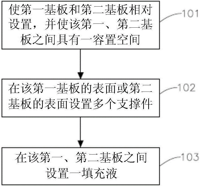
[0084] Please refer to figure 1 Shown is a basic flow chart of the bonding method of the present invention, which comprises the following steps:

[0085] Arranging a first substrate and a second substrate facing each other, and providing an accommodating space (101) between the first and second substrates;

[0086] setting a plurality of supports (102) on the surface of...


PUM


Abstract

The present invention provides a touch control panel, a touch control module and a laminating method therefor. In the main, a first substrate and a second substrate are disposed opposite to each other, and an accommodating space is formed between the first substrate and the second substrate. The accommodating space is filled with a filling solution and is provided with a plurality of support members. The supporting means between the first substrate and the second substrate is formed by the filing solution and the support members. Based on the above technique, no bubble is generated during the curing process after the laminating process. Therefore, the lamination yield is significantly improved. Meanwhile, the optical property of the above lamination technique is superior to that of the OGS full lamination technique. In addition, due to the effective supporting means formed between the first substrate and the second substrate, the deflection and derived flexible curved interference problem can be effectively solved.

Description

technical field [0001] The present invention relates to a touch panel, a touch module and a laminating method thereof, in particular to a related technology which can effectively improve the optical properties of a touch element bonded by glue and solve the problem of its deflection interference. Background technique [0002] The so-called bonding refers to the bonding technology between the liquid crystal panel (LCD) and the touch panel (TP). There are two main types of existing bonding technologies, namely direct bonding and direct bonding; one of the existing full bonding methods is as follows: [0003] Such as Figure 7A As shown, it is mainly to put a frame glue 71 on one side of a liquid crystal panel 70, and then pre-cure (PreCu) the frame glue 71 on the liquid crystal panel 70; [0004] Point water glue 72 in the pre-cured frame glue 71 (such as Figure 7B shown); [0005] Then a touch panel 80 is pasted on the liquid crystal panel 70 (such as Figure 7C shown), ...

Claims


Application Information

Patent Timeline
Patent Type & Authority Applications(China)
IPC IPC(8): G06F3/044
Inventor 柯淑茹黄子轩
Owner ELAN MICROELECTRONICS CORPORATION
Learn More