Method used for detecting display panel

A technology for display panels and array substrates, applied in static indicators, semiconductor/solid-state device testing/measurement, instruments, etc., can solve the problems of complex detection process, high cost, and high cost of display panels, so as to improve detection efficiency and simplify the detection process , the effect of reducing complexity

Active Publication Date: 2015-07-29
BOE TECH GRP CO LTD
View PDF10 Cites 11 Cited by
  • Summary
  • Abstract
  • Description
  • Claims
  • Application Information

AI Technical Summary

Problems solved by technology

[0004] However, the production of the organic light-emitting layer requires a relatively high cost, thus resulting in a relatively high cost for the entire display panel detection process
At the same time, in the process of organic light-emitting layer, some kind of defect may also occur. This defect is difficult to distinguish from the defect generated in the process of array substrate, which makes the whole detection process complicated and is not conducive to array testing. The improvement of reliability

Method used


Image

  • Method used for detecting display panel
  • Method used for detecting display panel
  • Method used for detecting display panel

Examples


Embodiment Construction

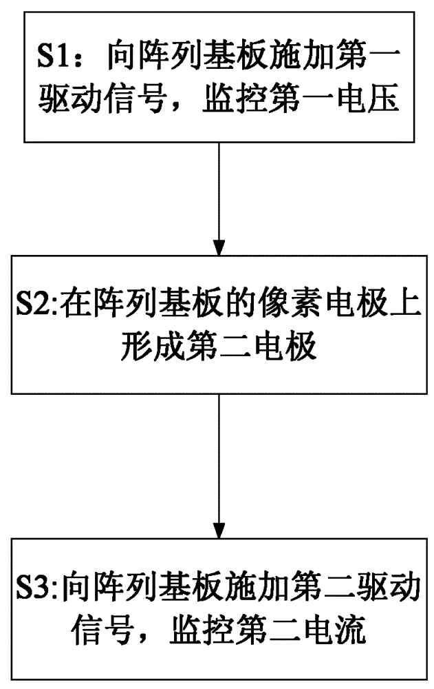
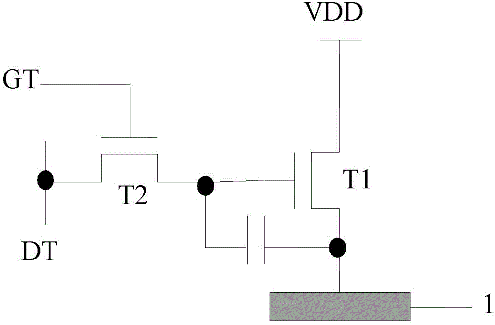
[0025] The embodiments described herein are mainly aimed at methods for testing a display panel. The display panel may include an array substrate for driving electroluminescent devices, and the array substrate may include pixel electrodes arranged in an array and a pixel switch array for driving the pixel electrodes. . The electroluminescence device may be various light emitting devices suitable for use as a pixel unit of a display panel, including but not limited to various LED devices, for example, organic light emitting diodes (OLEDs) and the like. In case the electroluminescent device is an OLED, the array substrate may be an AMOLED array substrate.

[0026] In order to clearly and conveniently illustrate the principles and ideas of the present invention, in the following embodiments, the method for detecting a display panel proposed by the present invention will be described by taking the array substrate as an example of an AMOLED array substrate. Of course, the present i...


PUM


Abstract

The invention discloses a method used for detecting a display panel. The display panel comprises an array substrate used for driving an electroluminescent device, wherein the array substrate comprises pixel electrodes arranged in an array and a pixel switch array used for driving the pixel electrodes. The method comprises the following steps: S1) applying a first driving signal to the manufactured array substrate, and monitoring first voltage on the pixel arrays; S2) forming a second electrode on each pixel electrode of the array substrate; S3) applying a second driving signal to the array substrate on which the second electrode is formed, and monitoring second current which flows the second electrode, wherein each pixel electrode is one of the cathode and the anode of the electroluminescent device, and each second electrode is the other one of the cathode and the anode of the electroluminescent device. According to the method, an organic luminescent layer does not need to be manufactured, and therefore, the cost of the whole detection process is greatly lowered. Meanwhile, interference brought by new defects which may be introduced in the manufacture of the organic luminescent layer is eliminated, a detection process of the display panel is simplified, detection complexity is lowered, and the method is favorable for improving detection efficiency.

Description

technical field [0001] The invention relates to the field of display technology, in particular to a method for detecting a display panel. Background technique [0002] The manufacture of the display panel of the display device generally includes multiple processes. For example, the manufacture of AMOLED display panels generally includes an array substrate (backplane) process, an organic light-emitting layer (EL) process, and a packaging process. In the array substrate manufacturing process, an array test (array test) process is usually used to screen the manufactured array substrate for defects to determine whether it has defects. On the one hand, it can intercept defective array substrates from flowing into subsequent manufacturing processes to produce defective display panels; on the other hand, it can monitor the stability of the array substrate manufacturing process. [0003] In order to verify the reliability of the array test (array test), it is usually necessary to ...

Claims


Application Information

Patent Timeline
Patent Type & Authority Applications(China)
IPC IPC(8): G09G3/00G09G3/32
CPCG09G3/006G09G3/3233G09G3/325G09G3/3266G09G3/3291G09G2300/043G09G2300/0809H01L22/14
Inventor 曹昆吴仲远
Owner BOE TECH GRP CO LTD
Why Eureka
Try Eureka