
Display device, gate driving circuit and driving method of gate driving circuit

A gate drive circuit and voltage terminal technology, applied to static indicators, static memory, instruments, etc., can solve problems such as prolonging blanking time and insufficient charging of pixel units

Active Publication Date: 2015-09-09
BOE TECH GRP CO LTD +1
View PDF4 Cites 47 Cited by
  • Summary
  • Abstract
  • Description
  • Claims
  • Application Information

AI Technical Summary

Problems solved by technology

[0008] Embodiments of the present invention provide a gate drive circuit, its drive method, and a display device, which can solve the problem of insufficient charging of pixel units due to prolonged blanking time

Method used


Image

  • Display device, gate driving circuit and driving method of gate driving circuit
  • Display device, gate driving circuit and driving method of gate driving circuit
  • Display device, gate driving circuit and driving method of gate driving circuit

Examples


Embodiment 1

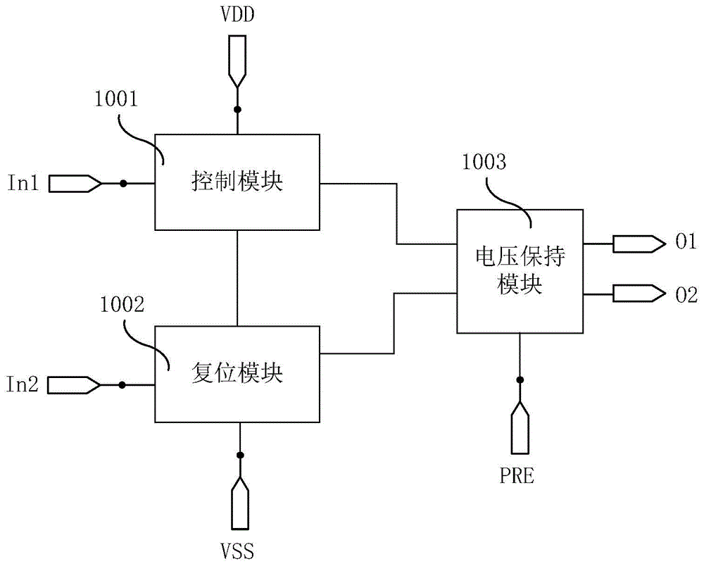
[0056] Such as Figure 4 As shown, the control module 1001 may include: a first transistor M1, the gate of which is connected to the first signal input terminal In1, the first pole is connected to the first voltage terminal VDD, and the second pole is connected to the reset module 1002 and the voltage holding module 1003 .

[0057] The reset module 1002 may include: a second transistor M2, the gate of which is connected to the second signal input terminal In2, the first pole is connected to the second voltage terminal VSS, and the second pole is connected to the control module 1001 and the voltage holding module 1003 .

[0058] When the compensation voltage terminal PRE includes the first compensation voltage terminal PRE1 and the second compensation voltage terminal PRE2; ​​the voltage holding module 1003 may include: a third transistor M3, a fourth transistor M4, a first capacitor C1 and a second capacitor C2.

[0059] The gate of the third transistor M3 is connected to the ...

Embodiment 2

[0073] This embodiment has the same structure as the control module 1001 and the reset module 1002 provided in the first embodiment. The difference is that the compensation voltage terminal includes the first compensation voltage terminal PRE1 and the second compensation voltage terminal PRE2; ​​the voltage holding module 1003 is as Figure 6 As shown, it may include: a fifth transistor M5, a sixth transistor M6 and a third capacitor C3.

[0074] Wherein, the gate of the fifth transistor M5 is connected to the control module 1001 and the reset module 1002, the first pole is connected to the first compensation voltage terminal PRE1, and the second pole is connected to the first signal output terminal O1. When the structures of the control module 1001 and the reset module 1002 are as above, the gate of the fifth transistor M5 is connected to the second electrodes of the first transistor M1 and the second transistor M2.

[0075] The gate of the sixth transistor M6 is connected t...

Embodiment 3

[0079] This embodiment is the same as the structure of the control module 1001 and the reset module 1002 provided in the first embodiment, the difference is that it includes a compensation voltage terminal, that is, the third compensation voltage terminal PRE3; the voltage holding module 1003 is as Figure 7 As shown, it may include: a seventh transistor M7 and a fourth capacitor C4.

[0080] The gate of the seventh transistor M7 is connected to the control module 1001 and the reset module 1002, the first pole is connected to the third compensation voltage terminal PRE3, and the second pole is connected to the first signal output terminal O1 and the second signal output terminal O2. When the structures of the control module 1001 and the reset module 1002 are as above, the gate of the seventh transistor M7 is connected to the second electrodes of the first transistor M1 and the second transistor M2.

[0081] One end of the fourth capacitor C4 is connected to the gate of the seven...


PUM


Abstract

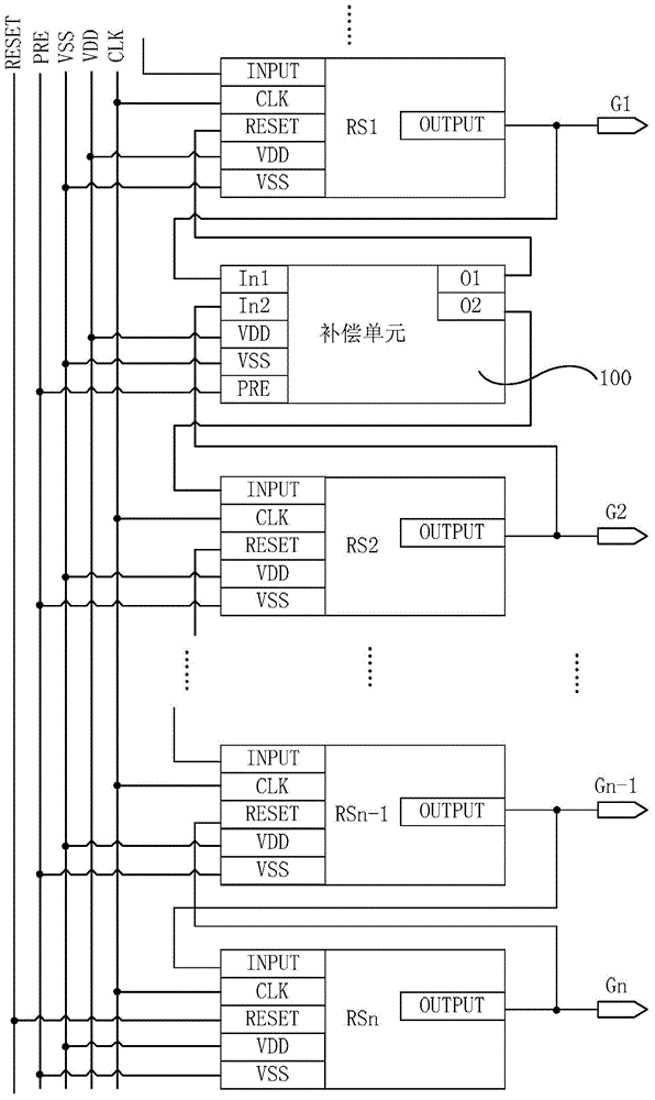
An embodiment of the invention provides a display device, a gate driving circuit and a driving method of the gate driving circuit and relates to the technical field of displaying. The gate driving circuit comprises at least two stages of shifting register units and at least one compensating unit, each compensating unit is arranged between every two adjacent shifting register units, the scanning signal output ends of first shifting register units are connected with the first signal input ends of the compensating units, the first signal output ends of the compensating units are connected with the reset signal ends of the first shifting register units, the scanning signal output ends of second shifting register units are connected with the second signal input ends of the compensating units, the second signal output ends of the compensating units are connected with the control signal input ends of the second shifting register units, and the compensating units are connected with at least one compensating voltage end, a first voltage end and a second voltage end. The display device, the gate driving circuit and the driving method of the gate driving circuit have the advantages that gate scanning signals can be compensated during blanking time, and the problem that a pixel unit cannot be charged fully since the blanking time is prolonged can be solved.

Description

technical field [0001] The invention relates to the field of display technology, in particular to a gate driving circuit, a driving method thereof, and a display device. Background technique [0002] Liquid Crystal Display (LCD for short) has the advantages of low radiation, small size, and low energy consumption, and is widely used in electronic products such as tablet computers, televisions, and mobile phones. The display screen of the liquid crystal display is provided with pixel units defined by a plurality of grid lines and data lines crossing horizontally and vertically. During the display process, the gate driving circuit can scan the gate lines row by row, and the data driving circuit can charge the pixel units through the data lines. [0003] In order to further reduce the production cost of liquid crystal display products, the existing gate drive circuit often adopts GOA (Gate Driver on Array, array substrate row drive) design to integrate TFT (Thin Film Transisto...

Claims


Application Information

Patent Timeline
Patent Type & Authority Applications(China)
IPC IPC(8): G09G3/36G09G3/20
CPCG09G3/3677G09G2310/0286G09G2354/00G11C19/28G09G3/3696G09G2300/0809G09G2310/0248G09G2310/061
Inventor 马磊陈希
Owner BOE TECH GRP CO LTD
Learn More