Semiconductor device etching method and semiconductor device formation method

A semiconductor and etching technology, which is applied in the direction of semiconductor devices, semiconductor/solid-state device manufacturing, electric solid-state devices, etc., can solve the problems of poor etch adjustability and achieve the effect of increasing the adjustable range

Active Publication Date: 2015-09-09
CSMC TECH FAB2 CO LTD
View PDF5 Cites 3 Cited by
  • Summary
  • Abstract
  • Description
  • Claims
  • Application Information

AI Technical Summary

Problems solved by technology

[0004] In view of the above-mentioned shortcomings of the prior art, the object of the present invention is to provide a semiconductor device etching method and forming method to solve the above-mentioned problem of poor etch adjustability

Method used


Image

  • Semiconductor device etching method and semiconductor device formation method
  • Semiconductor device etching method and semiconductor device formation method
  • Semiconductor device etching method and semiconductor device formation method

Examples


Embodiment Construction

[0018] Embodiments of the present invention are described below through specific examples, and those skilled in the art can easily understand other advantages and effects of the present invention from the content disclosed in this specification. The present invention can also be implemented or applied through other different specific implementation modes, and various modifications or changes can be made to the details in this specification based on different viewpoints and applications without departing from the spirit of the present invention.

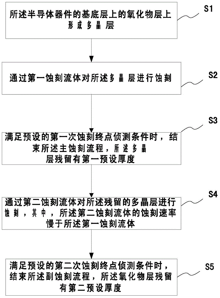
[0019] see figure 1 , The present invention provides a method for etching a semiconductor device, including: a main etching process and a secondary etching process.

[0020] The main etching process includes:

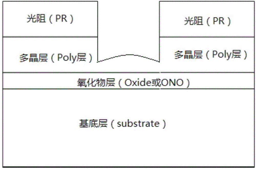
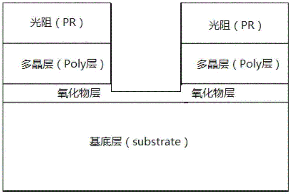
[0021] Step S1: Forming a polycrystalline layer by etching on the oxide layer on the substrate of the semiconductor device; in this embodiment, the semiconductor device is made of polycrystalline silicon, and the polycrystalli...


PUM


Abstract

The invention provides a semiconductor device etching method and a semiconductor device formation method. The semiconductor device etching method comprises a main etching process and at least one auxiliary etching process. The main etching process comprises steps of forming a polycrystal layer on an oxide layer on a stratum basale of a semiconductor device, performing etching on the polycrystal layer through a first etching fluid, and finishing the main etching flow and leaving a first preset thickness on the polycrystal layer when a preset first etching end point detection condition is met. The auxiliary etching process comprises steps of performing the etching on the residual polycrystal layer through a second etching fluid, wherein the etching speed of the second etching fluid is slower than that of the first etching fluid, finishing the auxiliary etching process when the preset second etching end point detection condition is met and leaving a second preset thickness on the oxide layer. The semiconductor device etching method increases the adjustable range of the etching amount of the oxide layer without changing the main etching process, and the adjustment of the thickness of the lower oxide layer does not affect the etching feature.

Description

technical field [0001] The invention relates to the technical field of semiconductor technology, in particular to a method for etching a semiconductor device and a method for forming a semiconductor device. Background technique [0002] In the polysilicon etching process, the main etching step (MainEtching) usually uses EPD (Etching Endpoint Detection) method plus a certain amount of overetching to ensure that the silicon is etched clean, and the etching characteristics of the main etching step also fix the oxide on the lower layer of the semiconductor device. The thickness of the layer (under-layerOxide or ONO). [0003] In the existing semiconductor manufacturing (FAB) etching process, although there is a function of adjusting the etching range of the oxide layer by adjusting the end point detection method, the adjustable range is too small and only (ie "Angstrom", 10 to the negative 10th power meter), very limited; and if the thickness of the oxide layer is adjusted by ...

Claims


Application Information

Patent Timeline
Patent Type & Authority Applications(China)
IPC IPC(8): H01L21/311H01L21/8247
CPCH01L21/31116H10B41/00
Inventor 华强周耀辉
Owner CSMC TECH FAB2 CO LTD
Why Eureka
Try Eureka