Double-active layer structured zinc oxide-based thin film transistor and preparation method thereof

A thin film transistor, zinc oxide thin film technology, applied in transistors, semiconductor devices, electrical components, etc., can solve the problems of high off-state current, low switching current, high carrier concentration, etc. Off-state current, the effect of improving light transmittance

Inactive Publication Date: 2015-09-09
SOUTH CHINA UNIV OF TECH
View PDF3 Cites 5 Cited by
  • Summary
  • Abstract
  • Description
  • Claims
  • Application Information

AI Technical Summary

Problems solved by technology

At present, one of the main problems of zinc oxide thin film transistors is that the generated semiconductor channel layer often has a high carrier concentration, which makes the off-state current of the device high and the switching current relatively low.

Method used


Image

  • Double-active layer structured zinc oxide-based thin film transistor and preparation method thereof
  • Double-active layer structured zinc oxide-based thin film transistor and preparation method thereof
  • Double-active layer structured zinc oxide-based thin film transistor and preparation method thereof

Examples


Embodiment

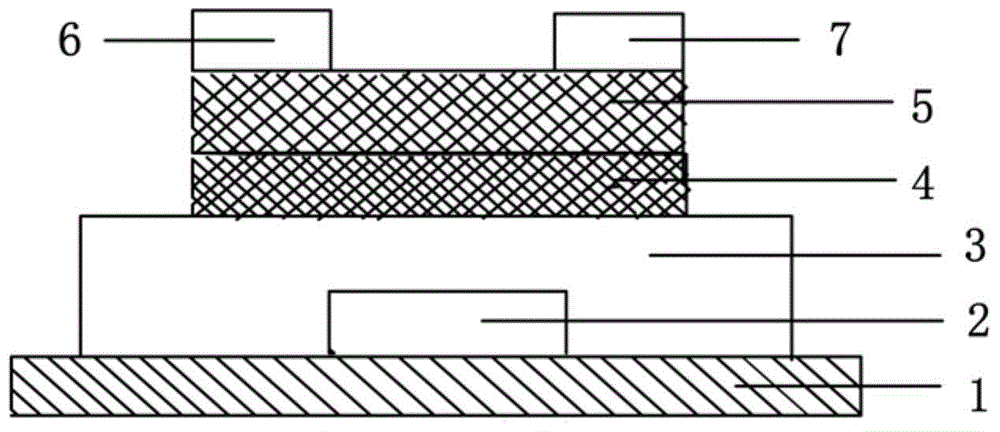
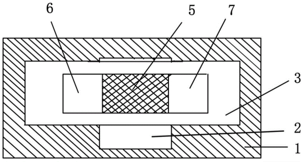
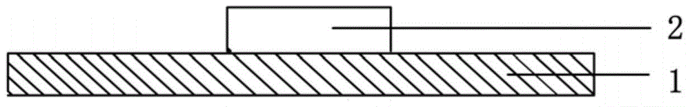
[0037] The zinc oxide-based thin film transistor with a dual active layer structure in this embodiment includes a substrate 1, a gate 2, a gate insulating dielectric layer 3, a first zinc oxide-based semiconductor active layer 4, and a second zinc oxide-based semiconductor active layer from bottom to top. A semiconductor active layer 5; the second zinc oxide-based semiconductor active layer is provided with a source electrode 6 and a drain electrode 7, and the source electrode 6 and the drain electrode 7 are located at both ends of the second semiconductor active layer 5; the The resistance value of the second zinc oxide-based semiconductor active layer is higher than that of the first zinc oxide-based semiconductor active layer, and the areas of the two active layers are equal.

[0038] The substrate in this embodiment may be a glass substrate or a plastic substrate.

[0039] The first zinc oxide-based semiconductor active layer in this embodiment can be an undoped zinc oxide...


PUM

PropertyMeasurementUnit
thicknessaaaaaaaaaa
thicknessaaaaaaaaaa

Abstract

The invention discloses a double-active layer structured zinc oxide-based thin film transistor. The double-active layer structure zinc oxide-based thin film transistor includes a substrate, a gate, a gate insulating dielectric layer, a first zinc oxide-based semiconductor active layer, a second zinc oxide-based semiconductor active layer, a source electrode and a drain electrode; the gate is formed on the substrate; the gate insulating dielectric layer covers the gate and the substrate; the active layers are formed on the gate insulating dielectric layer; the source electrode and the drain electrode are arranged on the second zinc oxide-based semiconductor active layer; the doping element of the first zinc oxide-based semiconductor active layer is one or two kinds of elements selected from Ga, Al, Hf, In and Sn; the second zinc oxide-based semiconductor active layer is a silicon-doped zinc oxide thin film; and the resistance value of the second zinc oxide-based semiconductor active layer is higher than that of the first zinc oxide-based semiconductor active layer. With the above technical scheme of the invention adopted, the zinc oxide-based thin film transistor has the advantages of effectively-decreased off-state current, improved on-off current ratio, improved light transmission performance in a visible light range, and improved stability.

Description

technical field [0001] The invention relates to the technical field of flat panel display driving, in particular to a zinc oxide-based thin film transistor with a double active layer structure and a preparation method thereof. Background technique [0002] Thin-film transistor (TFT) is a key component in the field of flat-panel display technology. In the last century, silicon-based thin-film transistors have been the mainstream core technology for active driving of flat-panel displays. Since the beginning of this century, with the rapid development of flat panel display technology, due to the low mobility of amorphous silicon TFT (0.5-1.0cm 2 / Vs) are limited in high-resolution displays. Although polysilicon TFT has high mobility, it has disadvantages such as complex process, expensive manufacturing cost, and difficulty in realizing large area, which restrict its market space. More importantly, silicon is a semiconductor with a narrow energy gap. Silicon-based TFTs are sen...

Claims


Application Information

Patent Timeline
Patent Type & Authority Applications(China)
IPC IPC(8): H01L29/786
CPCH01L29/7869
Inventor 刘玉荣姚若河耿魁伟
Owner SOUTH CHINA UNIV OF TECH
Why Eureka
Try Eureka