Supercharge Your Innovation With Domain-Expert AI Agents!

OLED micro-cavity structure and method of making

A microcavity and cavity electrode technology, which is applied in the direction of final product manufacturing, sustainable manufacturing/processing, semiconductor/solid-state device manufacturing, etc., can solve the problems of short circuit in adjacent pixel areas and leaving residues, etc.

Active Publication Date: 2015-09-09
LG DISPLAY CO LTD
View PDF11 Cites 20 Cited by
  • Summary
  • Abstract
  • Description
  • Claims
  • Application Information

AI Technical Summary

Problems solved by technology

Furthermore, it is not possible to well define the emissive layer using fine metal mask evaporation techniques
Moreover, the patterning of the transparent anode electrode in the prior art may result in leaving residues that may cause short circuits between adjacent pixel regions

Method used


Image

  • OLED micro-cavity structure and method of making
  • OLED micro-cavity structure and method of making
  • OLED micro-cavity structure and method of making

Examples


Embodiment Construction

[0040] Reference will now be made in detail to the preferred embodiments of the present invention, examples of which are illustrated in the accompanying drawings. However, this invention may be embodied in many different forms and should not be construed as limited to the embodiments set forth herein; rather, these embodiments are provided so that this disclosure will be thorough and complete, and will The idea of ​​the invention conveys to those skilled in the art. In the drawings, the thicknesses of layers and regions are exaggerated for clarity. Like reference numbers in the drawings indicate like elements.

[0041] It will also be understood that when a layer is referred to as being "on" another layer or substrate, it can be directly on the other layer or substrate, or intervening layers may also be present. In contrast, when an element is referred to as being "directly on" another element, there are no intervening elements present.

[0042] Throughout the specification...


PUM


Abstract

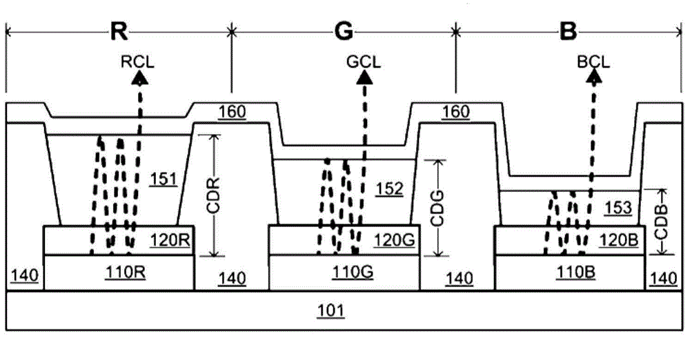
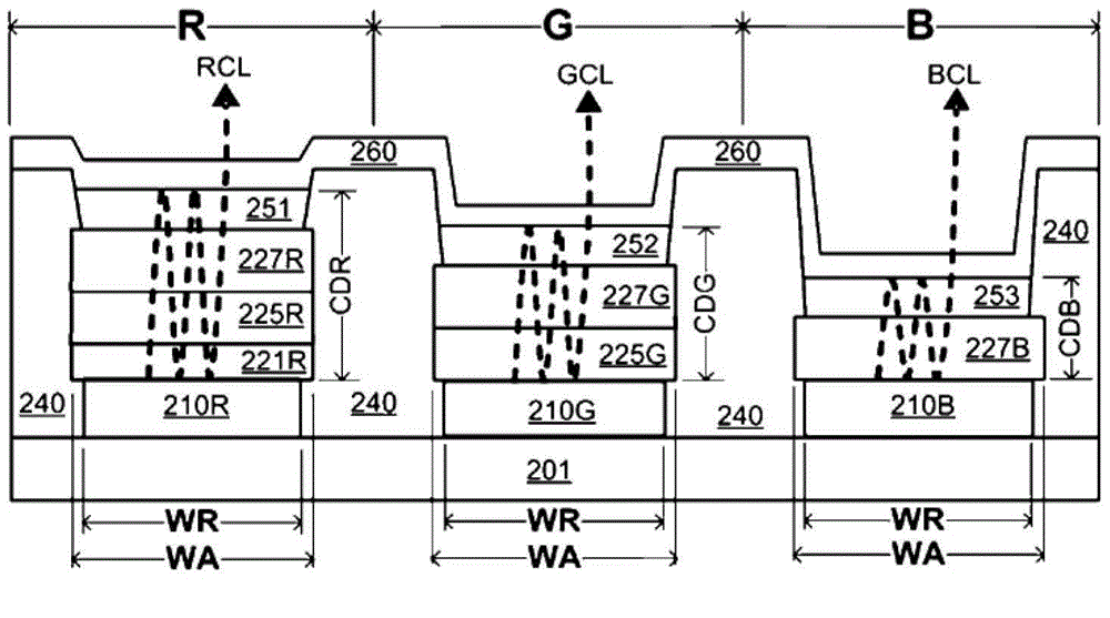
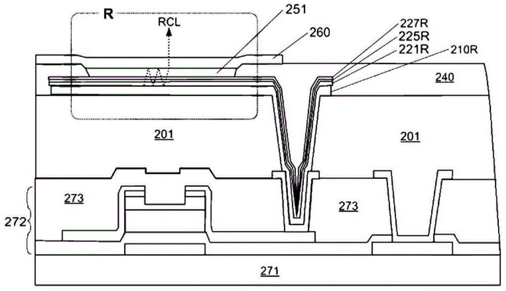
An organic light emitting diode, including: a substrate; a first cavity electrode in a first micro-cavity region of the substrate; a first transparent electrode of a first thickness in the first micro-cavity region, the first transparent electrode overlaps beyond a first side of the first cavity electrode; a first emissive layer in electrical connection with the first transparent electrode; and a cathode layer on the first emissive layer.

Description

technical field [0001] Embodiments of the present invention relate to organic light emitting diodes, and more particularly, to organic light emitting diode microcavity structures and fabrication methods thereof. Although embodiments of the present invention are suitable for a wide range of applications, they are particularly suitable for matrix structures having at least three sub-pixel regions. Background technique [0002] Generally, organic electroluminescent (EL) devices (also referred to as organic light emitting diode devices or OLED devices) can emit light at predetermined color wavelengths. OLED devices include an anode for hole injection, a cathode for electron injection, and an organic emissive layer sandwiched between the anode and cathode to recombine holes and electrons to emit light. OLED devices can be stacked one on top of the other such that one emissive layer emits one color and the other emissive layer emits another color such that the colors combine to f...

Claims


Application Information

Patent Timeline
Patent Type & Authority Applications(China)
IPC IPC(8): H01L51/50H05B33/10
CPCH01L51/5265H01L51/5218H01L27/3206H01L51/56H01L51/5215H01L27/3213H01L51/5209H01L27/322H10K59/30H10K59/351H10K59/38H10K59/876H10K59/80517H10K59/80515H10K59/80518Y02E10/549Y02P70/50H10K59/1201H10K59/122H10K30/82H10K50/852H10K59/35H10K71/00H10K50/813H10K50/816H10K50/818
Inventor 沈成斌金世埈
Owner LG DISPLAY CO LTD
Features
  • R&D
  • Intellectual Property
  • Life Sciences
  • Materials
  • Tech Scout
  • Unparalleled Data Quality
  • Higher Quality Content
  • 60% Fewer Hallucinations
Learn More