
Package and method of manufacturing package

A technology of packaging and bonding parts, which is applied in semiconductor/solid-state device manufacturing, semiconductor/solid-state device parts, electrical components, etc., and can solve problems such as failure, delamination, and weak bonding of solder joints between molding compounds and substrates , to achieve the effect of avoiding easy stratification

Inactive Publication Date: 2015-09-16
SAMSUNG SEMICON CHINA RES & DEV +1
View PDF4 Cites 0 Cited by
  • Summary
  • Abstract
  • Description
  • Claims
  • Application Information

AI Technical Summary

Problems solved by technology

Although this type of package can easily control the dimensional accuracy of the package, the bonding force between the molding compound and the solder joints of the substrate is weak, and delamination is easy to occur, resulting in failure

Method used


Image

  • Package and method of manufacturing package
  • Package and method of manufacturing package
  • Package and method of manufacturing package

Examples


Embodiment Construction

[0030] Hereinafter, the inventive concept will be described in detail by explaining exemplary embodiments with reference to the accompanying drawings. However, the inventive concepts may be embodied in many different forms and should not be construed as limited to the embodiments set forth herein; rather, these embodiments are provided so that this disclosure will be thorough and complete, and will inform the present Those of ordinary skill in the art fully convey the inventive concept. In the drawings, the same reference numerals denote the same elements. Furthermore, various elements and regions are shown schematically. Accordingly, the inventive concepts are not limited to the relative sizes or distances shown in the figures. It will be understood that although the terms first, second, third etc. may be used herein to describe various elements, components, regions, layers and / or sections, these elements, components, regions, layers and / or sections should not limited by t...


PUM


Abstract

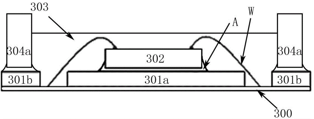
The invention provides a package and a method of manufacturing the package. The package includes a substrate, a first combining component, a second combining component, a chip, a blocking component and an encapsulation component; the substrate has a first surface and a second surface which backs on to the first surface; a plurality of pads are arranged in the substrate; the first combining component and the second combining component are arranged on the substrate; the second combining component is located around the first combining component; the chip is arranged on the first combining component and is electrically connected with the plurality of pads through leads; the blocking component is arranged on the second combining component; the encapsulation component is arranged at the inner side of the blocking component so as to encapsulate the chip, the first combining component and the leads.

Description

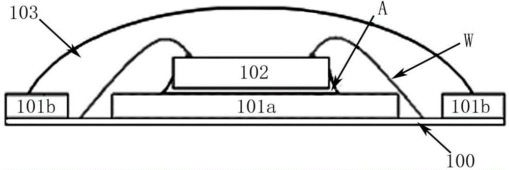
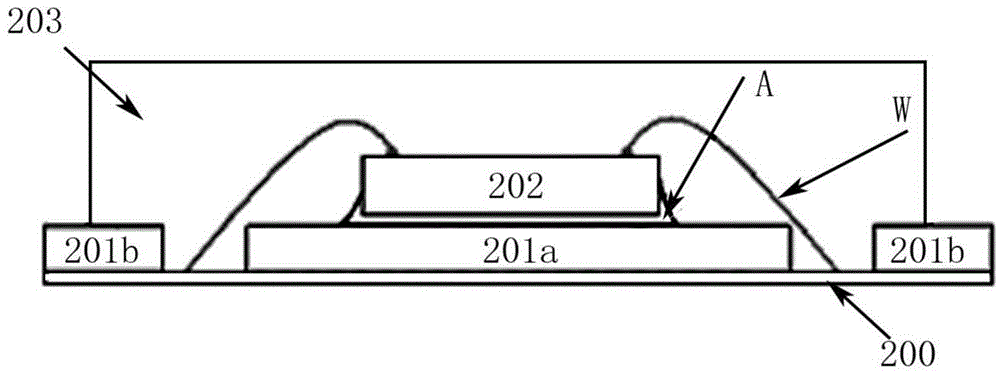
technical field [0001] The invention relates to the packaging field, in particular to a package and a method for manufacturing the package. Background technique [0002] Existing packaging technology usually adopts glue dispensing or molding to provide protection for the chip and prevent the chip from becoming invalid due to environmental impact and external force. [0003] figure 1 A schematic cross-sectional view of a dispensing package of the related art is shown, in which a chip 102 is disposed on a bonding member 101a through an adhesive layer A including a bonding agent, and a lead W is used to connect the chip 102 to a bonding pad disposed on a substrate 100. The pads (not shown) are electrically connected, and then encapsulated with the encapsulation member 103 by dispensing glue. Dispensing packaging is not easy to control the dimensional accuracy of the package. In addition, this type of package also has the disadvantage of low mechanical strength, so that it ca...

Claims


Application Information

Patent Timeline
IPC IPC(8): H01L23/10H01L23/31H01L21/56
CPCH01L23/49855H01L24/29H01L24/32H01L24/48H01L24/73H01L24/92H01L23/16H01L23/24H01L23/3142H01L2224/2919H01L2224/32225H01L2224/32238H01L2224/73265H01L2224/48227H01L2224/48228H01L2224/48229H01L2924/00012H01L2224/92227H01L2924/15162H01L2924/00
Inventor 徐健
Owner SAMSUNG SEMICON CHINA RES & DEV
Learn More