Organic light emitting diode display panel, manufacturing method thereof and display

A technology of light-emitting diodes and display panels, which is applied in semiconductor/solid-state device manufacturing, electric solid-state devices, semiconductor devices, etc., and can solve stress and mechanical strength differences, OLED display panel laser sintering state differences, glass glue laser sintering state differences, etc. problem, achieve the effects of reducing temperature difference, uniform laser sintering state, and improving packaging performance

Inactive Publication Date: 2015-09-16
BOE TECH GRP CO LTD +1
View PDF5 Cites 14 Cited by
  • Summary
  • Abstract
  • Description
  • Claims
  • Application Information

AI Technical Summary

Problems solved by technology

The glass glue 13 inside the hole-digging area 11 cannot be subjected to the reflected laser light of the metal block 121 on both sides and the bottom layer and the inorganic protective layer 122 covered therewith, while the glass glue 13 in the metal area 12 can be subjected to the reflected laser light of the bottom metal block 121, thereby The temperature of the glass glue in the hole-digging area is slightly lower than that in other areas, so there is a difference in the laser si

Method used


Image

  • Organic light emitting diode display panel, manufacturing method thereof and display
  • Organic light emitting diode display panel, manufacturing method thereof and display
  • Organic light emitting diode display panel, manufacturing method thereof and display

Examples


Embodiment Construction

[0038] The following will clearly and completely describe the technical solutions in the embodiments of the present invention in conjunction with the accompanying drawings in the embodiments of the present invention. Obviously, the described embodiments are only some of the embodiments of the present invention, not all of them. Based on the embodiments of the present invention, all other embodiments obtained by persons of ordinary skill in the art without making creative efforts belong to the protection scope of the present invention.

[0039] The embodiment of the present invention provides an organic light emitting diode display panel and its manufacturing method, and the display, which is used to reduce the temperature difference between the glass glue in the hole-digging area and other areas when heated, so that the laser sintered state in the OLED display panel Uniformity, improve the overall encapsulation performance of the glass glue.

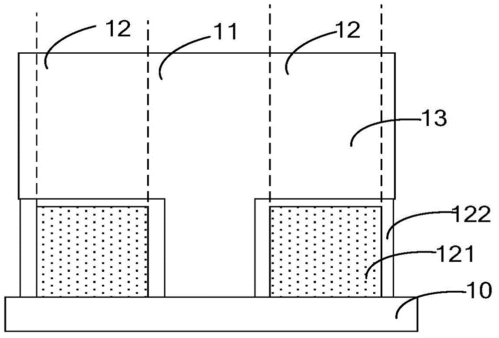
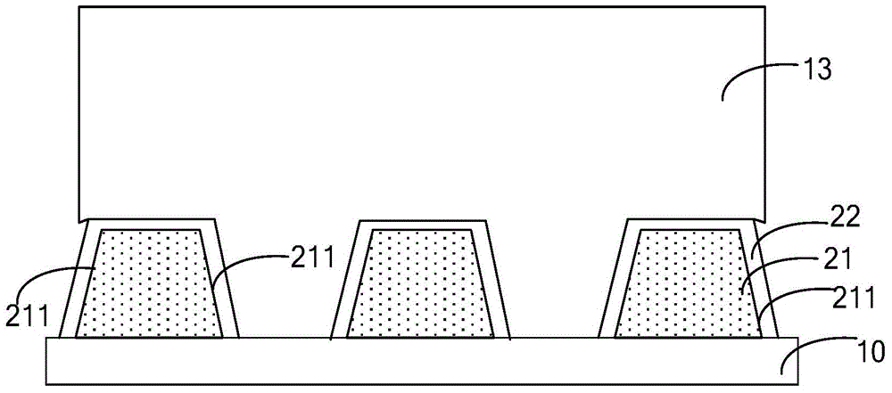
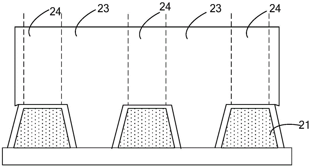
[0040] see figure 2 , a kind of...


PUM

PropertyMeasurementUnit
Angleaaaaaaaaaa

Abstract

The invention provides an organic light emitting diode OLED display panel, a manufacturing method thereof and a display. The temperature difference between heated glass cement of a dug area and heated glass cement of another area is reduced, so that uniform laser sintering state is realized in the OLED display panel. The overall package performance of the glass cement is improved. The OLED display panel comprises back plate glass, cover plate glass, and glass cement located between the back plate glass and the cover plate glass and a number of metal blocks. Each metal block is covered by an inorganic protective layer. A dug area is arranged between two adjacent metal blocks. The glass cement contacts the back plate glass through the dug area. The OLED display panel is characterized in that at least one metal block and the inorganic protective layer which covers the metal block have a surface which reflects incident laser into a dug area.

Description

technical field [0001] The invention relates to the technical field of displays, in particular to an organic light emitting diode display panel, a manufacturing method thereof, and a display. Background technique [0002] An organic light-emitting diode (Organic Light-Emitting Diode, OLED for short) display is also called an organic electro-laser display. An OLED device is a display device that drives a luminescent material to emit light autonomously by an electric current. OLED needs to ensure the long-term normal operation of the internal device structure through good sealing. The prior art usually adopts glass glue (Frit) packaging technology, wherein the laser sintering process plays a key role in the sealing performance of the glass glue. [0003] In the prior art, a large piece of metal is designed under the glass glue coating area and a hole is designed on the big piece of metal to ensure that the glass glue can be in direct contact with the backplane glass during t...

Claims


Application Information

Patent Timeline
IPC IPC(8): H01L27/32H01L51/52H01L51/56
CPCH10K50/8423H10K50/8426H10K50/856H10K50/8428H10K71/00
Inventor 肖昂
Owner BOE TECH GRP CO LTD
Why Eureka
Try Eureka