Photocoupler
A technology of optical coupling device and light receiving element, which is applied in the direction of semiconductor devices, electrical components, circuits, etc., can solve the problem of increasing the size of the installed circuit board, and achieve the effect of reducing the size
- Summary
- Abstract
- Description
- Claims
- Application Information
AI Technical Summary
Problems solved by technology
Method used
Image

Examples
no. 1 approach
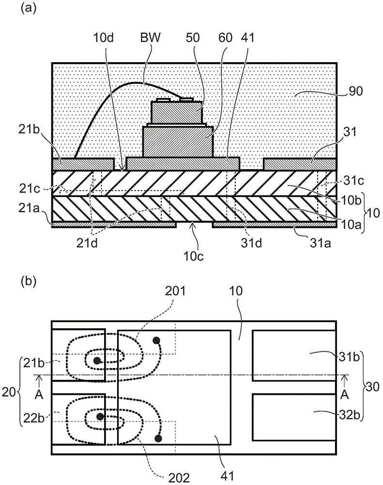
[0024] figure 1 (a) is a schematic sectional view of the optical coupling device according to the first embodiment, figure 1 (b) is a schematic plan view of a mounting substrate provided with a conductive pattern on an insulating substrate.
[0025] The optical coupling device has an insulating substrate 10 , an input terminal 20 , an output terminal 30 , a (first) lower pad portion 41 , a light receiving element 60 , and a light emitting element 50 .
[0026] figure 1 (a) is along figure 1 A schematic sectional view of line A1-A2 of (b). The insulating substrate 10 has a first layer 10a and a second layer 10b, the lower surface of the first layer 10a is defined as a first surface 10c, and the upper surface of the second layer 10b is defined as a second surface 10d. A plurality of through holes are provided on the insulating substrate 10 .
[0027] The input terminal 20 has a first terminal 21 and a second terminal 22 . The first terminal 21 has: a first conductive regio...
no. 2 approach
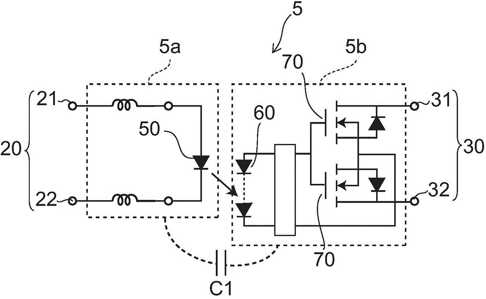
[0045] Figure 5 (a) is a schematic sectional view of the optical coupling device according to the second embodiment, Figure 5 (b) is a schematic plan view of a mounting substrate provided with a conductive pattern on an insulating substrate.
[0046] The optical coupling device has an insulating substrate 10 , an input terminal 20 , an output terminal 30 , an underlayment portion 41 , a light receiving element 60 , and a light emitting element 50 .
[0047] The insulating substrate 10 has a first layer 10a, a second layer 10b, and a third layer 10c. The lower surface of the first layer 10a is a first surface 10c, and the upper surface of the second layer 10b is a second surface 10d. A plurality of through holes are provided on the insulating substrate 10 .
[0048] The first spiral conductive region 201 is disposed between the first layer 10a and the third layer 10c, and is respectively connected to the first conductive region 21a and the second conductive region 21b of th...
no. 3 approach
[0053] Figure 7 (a) is a schematic perspective view of an optical coupling device according to a third embodiment, Figure 7 (b) is a schematic sectional view, Figure 7 (c) is a schematic plan view before molding the sealing resin layer.
[0054] The optical coupling device has an insulating substrate 10 , an input terminal 20 , an output terminal 30 , a first underlayment portion 41 , a second underlayment portion 40 , a light receiving element 60 , a resistor 90 , a light emitting element 50 and a MOSFET 70 . also, Figure 7 (b) is a schematic cross-sectional view along line A2-A2.
[0055] The insulating substrate 10 has a first face 10a and a second face 10b. The input terminal 20 has a first terminal 21 and a second terminal 22 . The first terminal 21 has a first conductive region 21a provided on the first face 10a and a second conductive region 21b provided on the second face 10b. The second terminal 22 has a first conductive region 22a disposed on the first face...
PUM
 Abstract
Description
Claims
Application Information
PatSnap Eureka turns technology decisions into work you can execute. Powered by our Innovation Knowledge Graph, it runs expert workflows across engineering, life sciences, materials and intellectual property. Get your review-ready output in minutes.


