Drain electrode modulation circuit for GaN microwave power amplifier

A drain modulation, microwave power technology, applied in power amplifiers, amplifier protection circuit layout, improving amplifiers to improve efficiency, etc., can solve the problems of delay not meeting the requirements of the index, tailing, slow switching speed, etc., to improve the overall Power efficiency, the effect of solving voltage overshoot, and avoiding burnout

Active Publication Date: 2015-09-16
江苏博普电子科技有限责任公司
View PDF4 Cites 12 Cited by
  • Summary
  • Abstract
  • Description
  • Claims
  • Application Information

AI Technical Summary

Problems solved by technology

The working voltage of the GaN power microwave amplifier can reach 28~50V, which can be realized by using high-voltage PMOS transistors and discrete drive transistors. The main disadvantage of this implementation method is th

Method used


Image

  • Drain electrode modulation circuit for GaN microwave power amplifier
  • Drain electrode modulation circuit for GaN microwave power amplifier

Examples


Embodiment Construction

[0025] The present invention will be further described below in conjunction with the accompanying drawings. The following examples are only used to illustrate the technical solution of the present invention more clearly, but not to limit the protection scope of the present invention.

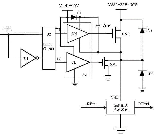
[0026] Such as figure 1 Shown is the schematic circuit diagram of the present invention: TTL is the input drain modulation signal, RFin is the input radio frequency signal of the GaN microwave pulse power amplifier, and the radio frequency signal can be a continuous wave or a pulse signal. The output signal of the GaN microwave pulse power amplifier is RFout. U1 is an inverter, and U2 is a logic circuit, which mainly implements adjustable signal delay and prevents the input signal HI of the high-end NMOS driver and the input signal LI of the low-end NMOS driver from being high at the same time. U3 is high-end NMOS and low-end NMOS tube drivers DH, DL. D1 is a bootstrap diode, Cboot is a boots...


PUM


Abstract

The invention discloses a drain electrode modulation circuit for a GaN microwave power amplifier. A modulation signal and an inverse-phase signal transmitted through a phase inverter are simultaneously input into a logic circuit, and a high-end NMOS driver input signal and a low-end NMOS driver input signal are output after delaying is performed. The high-end NMOS driver input signal and the low-end NMOS driver input signal are respectively input into a high-end NMOS driver and a low-end NMOS driver, the output end of the high-end NMOS driver and the output end of the low-end NMOS driver are respectively connected to a grid electrode of the high-end NMOS driver and a grid electrode of the low-end NMOS driver. A source electrode of a high-end NMOS tube serves as a drain electrode voltage end of the GaN microwave power amplifier. The phenomenon that the drain electrode voltage end of the GaN microwave power amplifier is low in discharging speed and accordingly trailing is caused is avoided by means of the drain electrode modulation circuit, the delay time for modulating the signals to the rising edge and falling edge of the drain electrode voltage end is shortened, and overshoot voltage amplitude of the drain electrode voltage end is reduced.

Description

technical field [0001] The invention relates to a drain modulation circuit for a GaN microwave power amplifier. Background technique [0002] Pulse modulation power amplifiers have been widely used in radar and many other communication systems. When the microwave pulse power amplifier is working, the input signal generally adopts radio frequency modulation signal, and at the same time directly modulates the power amplifier, that is, controls the working state and non-working state of the internal power tube of the power amplifier through an external TTL signal. Combined with radio frequency modulation and power amplifier direct modulation, it can effectively reduce the radar emission squelch level, improve the overall power supply efficiency of the radar, and protect the final high-power microwave devices. Direct modulation of the power amplifier adopts two modulation methods: gate modulation and drain modulation circuit. The gate modulation circuit is easy to implement, b...

Claims


Application Information

Patent Timeline
IPC IPC(8): H03F1/02H03F1/52H03F3/20
Inventor 沈美根陈强郑立荣肖清李贺关晓龙
Owner 江苏博普电子科技有限责任公司
Why Eureka
Try Eureka