Block erasing method for NAND type flash memory

A flash memory, the first-time technology, applied in static memory, read-only memory, information storage, etc., can solve the problems of increased programming interference, increased programming time, and reduced channel bootstrap efficiency, so as to reduce programming interference, The effect of saving programming time and increasing channel bootstrap efficiency

Inactive Publication Date: 2015-09-23
HEFEI HENGSHUO SEMICON CO LTD
View PDF6 Cites 6 Cited by
  • Summary
  • Abstract
  • Description
  • Claims
  • Application Information

AI Technical Summary

Problems solved by technology

[0006] Since the initial threshold voltage of each memory cell before the erase operation is different, and the speed at which the electrons in the floating gate of each memory cell tunnel to the channel is different, the erase operation is performed on the memory cells in the entire block together operation, so the storage unit with slow tunneling speed determines the time of the entire erase operation, which causes some memory units with fast erasing speed to be erased too deeply, so that after the erase verification succeeds, the The threshold voltage distribution of the memory cells is very wide, which will result in lower channel bootstrap efficiency for page programming operations, increased programming time, and increased program disturbance

Method used


Image

  • Block erasing method for NAND type flash memory
  • Block erasing method for NAND type flash memory
  • Block erasing method for NAND type flash memory

Examples


Embodiment Construction

[0032] In order to more clearly illustrate the technical solutions of the embodiments of the present invention, the following will briefly introduce the accompanying drawings that need to be used in the description of the embodiments. Obviously, the accompanying drawings in the following description are only some embodiments of the present invention. For Those of ordinary skill in the art can also obtain other drawings based on these drawings without making creative efforts.

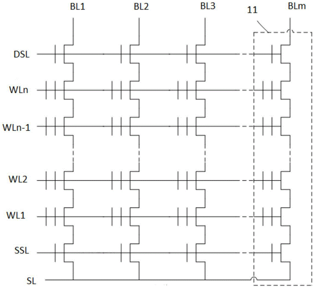
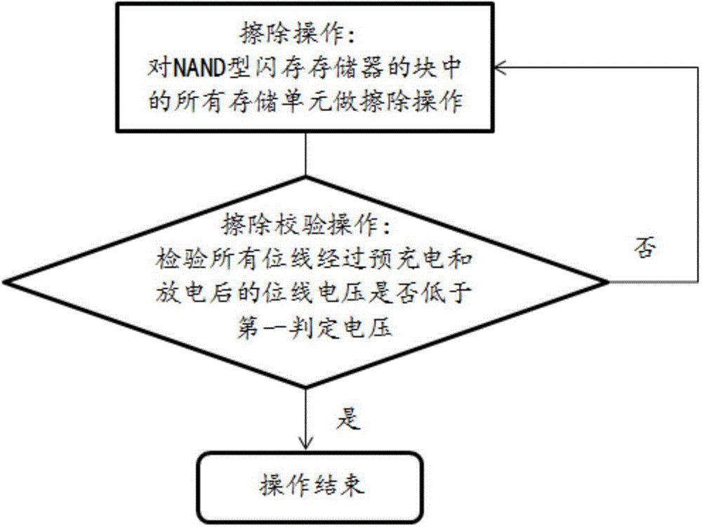
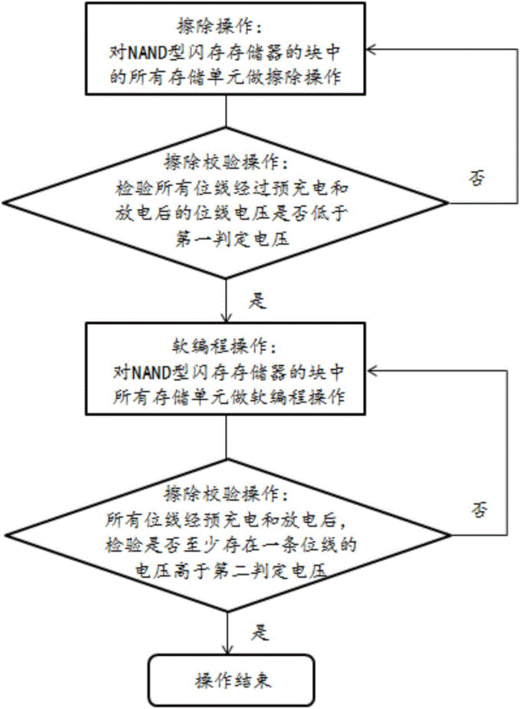
[0033] image 3 It is a flow chart of a block erasing method of a NAND flash memory provided by the present invention. next to figure 1 The block structure of shown NAND type flash memory memory is taken as an example to describe the block erasing method of a kind of NAND type flash memory memory of the present invention, as image 3 Shown, the block erasing method of NAND type flash memory memory of the present invention comprises the following steps:

[0034] Step one (201): erasing operation, all s...


PUM


Abstract

The invention discloses a block erasing method for a NAND type flash memory. The method comprises erasing operation, erasing examination operation, soft programming operation and soft programming examination operation. By means of soft programming operation, all memory cells of a block of the NAND type flash memory are programmed together, and time for programming the memory cells can be saved greatly. By means of soft programming examination operation, all the memory cells of the block of the NAND type flash memory are examined together, the operating mode of soft programming examination operation is identical with that of erasing examination operation, and soft programming examination operation is different from erasing examination operation only in bit line discharging time or examination judgment voltage. By the adoption of the method, the threshold voltage distribution of the memory units of the block of the NAND type flash memory can be made compact, sound initial threshold voltage distribution is provided for page programming operation, so that programming time is saved, the channel bootstrap efficiency of page programming operation is improved, and programming disturbance is reduced.

Description

technical field [0001] The invention relates to the field of NAND flash memories, in particular to a block erasing method for NAND flash memories. Background technique [0002] Flash memory is a type of non-volatile memory that retains information after power loss. Flash memories are classified into NOR flash memories and NAND flash memories according to the structure of storage cells in the array. NOR-type flash memory is an array formed in parallel, which has the advantage of fast random access speed, and is mainly used to store codes; while NAND-type flash memory is formed in series in an array, which has the advantage of small unit bit area and is used for storage massive data. The circuit diagram of the block structure of NAND flash memory is as follows figure 1 As shown, including n word lines (WL1, WL2, ..., WLn), m bit lines (BL1, BL2, ..., BLm), a source gate line (SSL), a drain gate line (DSL ) and a source line (SL), the part of the storage unit marked by the ...

Claims


Application Information

Patent Timeline
Patent Type & Authority Applications(China)
IPC IPC(8): G11C16/16
Inventor 刁静
Owner HEFEI HENGSHUO SEMICON CO LTD
Why Eureka
Try Eureka