Array substrate, method for manufacturing array substrate, and display device

An array substrate and manufacturing method technology, applied in the field of array substrate manufacturing, can solve the problems of decreased pixel aperture ratio, poor electrical conductivity, large channel length, etc., and achieve the effect of reducing the overall length

Active Publication Date: 2018-07-17
TCL CHINA STAR OPTOELECTRONICS TECH CO LTD
View PDF6 Cites 0 Cited by
  • Summary
  • Abstract
  • Description
  • Claims
  • Application Information

AI Technical Summary

Problems solved by technology

In the prior art, the array substrate includes gate lines and gate electrodes, semiconductor layers, source and drain electrodes, etch barrier layers, insulating layers, and pixel electrodes. The second metal layer must have a certain overlapping width with the etch barrier layer when forming the source and drain electrodes, so as to ensure that the second metal layer can completely cover the semiconductor layer when the manufacturing process deviates, so that the length of the channel formed by the semiconductor layer is relatively large. Poor conductivity, resulting in a decrease in pixel aperture ratio

Method used


Image

  • Array substrate, method for manufacturing array substrate, and display device
  • Array substrate, method for manufacturing array substrate, and display device
  • Array substrate, method for manufacturing array substrate, and display device

Examples


Embodiment Construction

[0033] The following will clearly and completely describe the technical solutions in the embodiments of the present invention with reference to the accompanying drawings in the embodiments of the present invention. Obviously, the described embodiments are only some, not all, embodiments of the present invention. Based on the embodiments of the present invention, all other embodiments obtained by persons of ordinary skill in the art without making creative efforts belong to the protection scope of the present invention.

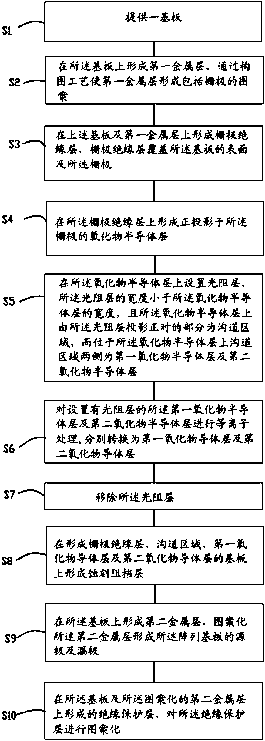
[0034] see figure 1 , which is a flowchart of a method for manufacturing an array substrate according to a preferred embodiment of the present invention. The array substrate belongs to oxide semiconductor structure transistors. Before elaborating the specific preparation method, it should be understood that in the present invention, the patterning refers to the patterning process, which may include a photomask process, or, include a photomask process and an e...


PUM


Abstract

The present invention provides a method for manufacturing an array substrate, which is characterized in that the method for manufacturing the array substrate includes: forming a first metal layer on the substrate, and making the first metal layer form a pattern including a gate through a patterning process; Forming a gate insulating layer on the substrate and the first metal layer, forming an oxide semiconductor layer projected onto the gate on the gate insulating layer; disposing a photoresist layer on the oxide semiconductor layer, On both sides of the channel region on the oxide semiconductor layer are the first oxide semiconductor layer and the second oxide semiconductor layer; for the first oxide semiconductor layer and the second oxide semiconductor layer provided with a photoresist layer The layer is subjected to plasma treatment to remove the photoresist layer; an etching stopper layer is formed on the substrate; a source electrode and a drain electrode are formed on the substrate, wherein the source electrode is in contact with the first oxide conductor layer, and the The drain is in contact with the second oxide conductor layer.

Description

technical field [0001] The present invention relates to the field of manufacturing array substrates, in particular to an array substrate, a method for manufacturing the array substrate and a display device. Background technique [0002] The currently widely used oxide array substrate uses oxide semiconductor as the active layer, which has the characteristics of high mobility, high on-state current, better switching characteristics, and better uniformity, and can be applied to applications that require fast response and large current , such as high-frequency, high-resolution, large-size displays, and organic light-emitting displays. In the prior art, the array substrate includes gate lines and gate electrodes, semiconductor layers, source and drain electrodes, etch barrier layers, insulating layers, and pixel electrodes. The second metal layer must have a certain overlapping width with the etch barrier layer when forming the source and drain electrodes, so as to ensure that ...

Claims


Application Information

Patent Timeline
Patent Type & Authority Patents(China)
IPC IPC(8): H01L21/77H01L21/46H01L27/12
CPCH01L21/46H01L21/77H01L27/12H01L27/1288H01L29/4908H01L29/66969H01L29/7869H01L27/1225H01L27/127H01L29/24H01L29/45H01L29/51H01L29/518
Inventor 李文辉
Owner TCL CHINA STAR OPTOELECTRONICS TECH CO LTD
Why Eureka
Try Eureka