

Schottky barrier high current density igbt device
A technology with high current density and Schottky potential, applied in the manufacture of electrical components, semiconductor devices, semiconductor/solid-state devices, etc., can solve the problem of weakening IGBT conductance modulation effect, achieve enhanced conductance modulation effect, and simple switch controllability , The effect of reducing the saturation pressure drop
- Summary
- Abstract
- Description
- Claims
- Application Information
AI Technical Summary
Problems solved by technology
Method used
Image

Examples
Embodiment Construction
[0029] The specific implementation manners of the present invention will be further described in detail below in conjunction with the accompanying drawings and embodiments. The following examples are used to illustrate the present invention, but are not intended to limit the scope of the present invention.
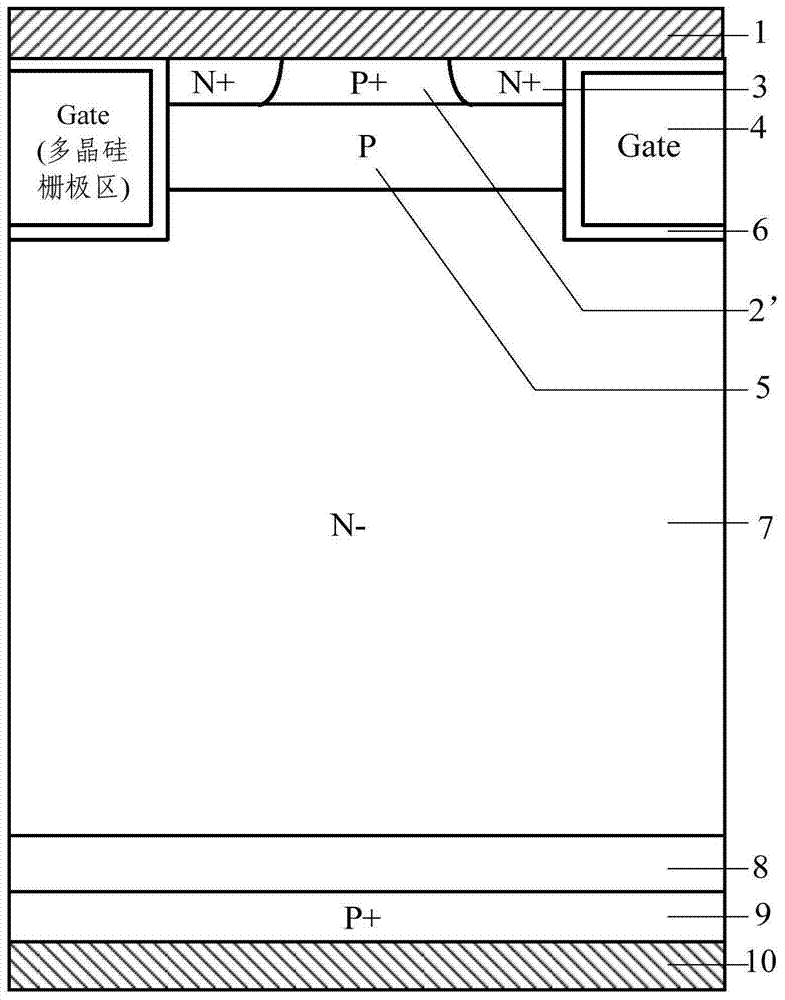
[0030] Known IGBT devices are generally composed of thousands of IGBT units connected in parallel, wherein the emitter, gate and collector of each unit cell are connected together through metal or polysilicon film. The chip area of each IGBT device along its peripheral edge is used as a fringe electric field stop region to ensure the breakdown voltage of the device.
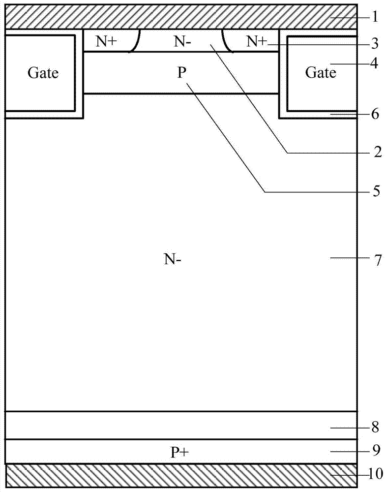
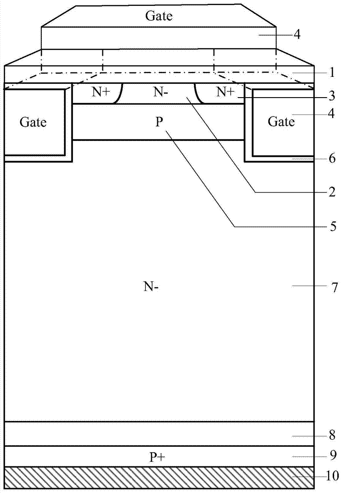
[0031] figure 1 A schematic diagram showing a two-dimensional cross-sectional cell structure of a typical IGBT device in the prior art, such as figure 1 As shown, the typical IGBT device includes: emitter metal region 1, P+ type region 2', N+ type doped source region 3, polysilicon gate region 4, P type b...
PUM
 Abstract
Description
Claims
Application Information