A kind of precharging circuit and photovoltaic inverter
A pre-charging circuit and photovoltaic inverter technology, which is applied in photovoltaic power generation, photovoltaic modules, electrical components, etc., can solve the problems of current impact and low DC bus pre-charging voltage, so as to avoid current impact and solve the problem of pre-charging voltage low effect
- Summary
- Abstract
- Description
- Claims
- Application Information
AI Technical Summary
Problems solved by technology
Method used
Image
Examples
example 1
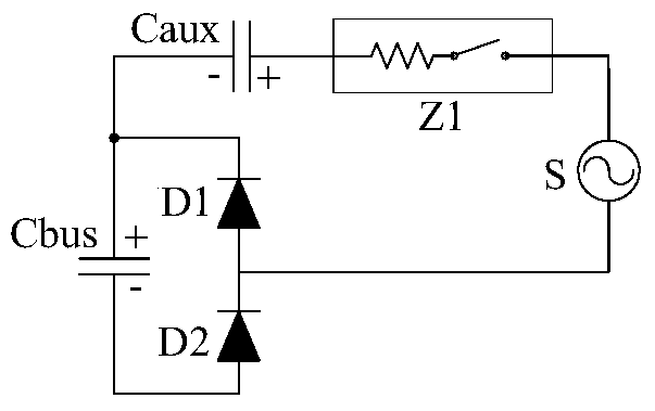
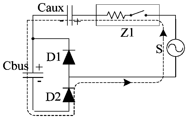
[0056] see Figure 2a , taking the pre-charging circuit with an AC power source S, a rectifying half-bridge formed by connecting diodes D1 and D2 in series, and an auxiliary charging capacitor Caux as an example (in the figure, Z1 indicates that the pre-charging circuit is connected in series The switch current limiting device on the only charging path; Cbus represents the target charging capacitor. After reaching the charging steady state, the voltage across the target charging capacitor is the DC bus pre-charging voltage): when the AC power supply S is at the forward voltage, the charging path Such as Figure 2b As shown, the current passes through Z1, Caux, Cbus, and D2 to form a charging loop, which charges Cbus and Caux positively; when the AC power supply S is at a negative voltage, the charging path is as follows: Figure 2c As shown, the current passes through D1, Caux, and Z1 to form a charging loop, and reversely charges Caux. Since Caux and Cbus are included in th...
example 2
[0067] see Figure 4a , taking the pre-charging circuit as an example with an AC power source S, a rectifying half-bridge formed by connecting diodes D1 and D2 in series, and two auxiliary charging capacitors Caux1~Caux2 (the switch current limiting device Z1 is connected in series to the charger where Caux1 is located) On the path, the switching current limiting device Z3 is connected in series on the charging path where Caux2 is located, and the switching current limiting device Z3 is connected in series on a section of the charging path shared by Caux1 and Caux2):
[0068] When the AC power supply S is at a forward voltage, there are two charging paths, such as Figure 4b As shown, one of the currents passes through Z2, D1, Cbus, Caux2, and Z3 to form a charging loop to charge Cbus and Caux2; the other current passes through Z2, D1, Caux1, and Z1 to form a charging loop to reversely charge Caux1. When the AC power supply S is at negative voltage, there are two charging pat...
example 3
[0079] In order to make the charging speed faster, the load capacity of the DC side of the inverter is stronger, and the three-phase power rectification can also be fully utilized. Such as Image 6 As shown, the pre-charging circuit includes 3 AC power sources, 3 rectifying half-bridges, 1 auxiliary charging capacitor Caux and 4 switching current limiting devices. Image 6 and Figure 2a The only difference is that the number of AC power supply and half-bridge rectification is increased, and the charging principle remains the same, refer to Figure 2b ~ Figure 2c related descriptions.
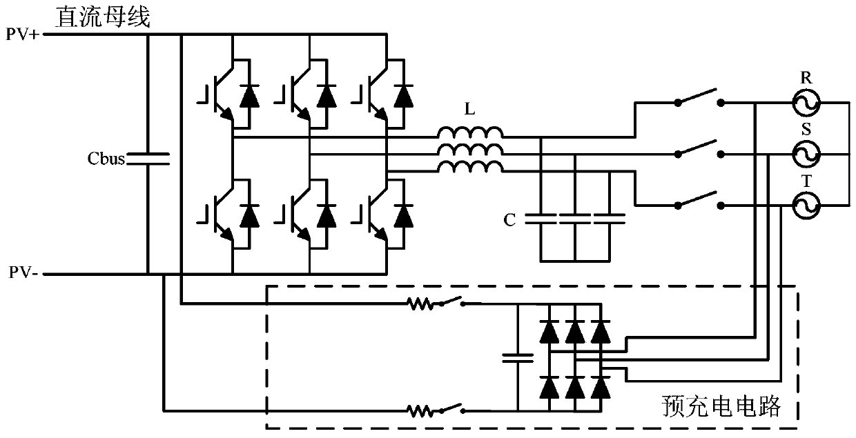
[0080] Will Image 6 The circuit shown is applied to the Figure 7 In the shown three-phase two-level photovoltaic inverter, the pre-charging function can be realized by adding additional auxiliary charging capacitor Caux1, three rectifying half-bridges and three switching current limiting devices Z1-Z3. Comparison figure 1 It can be seen that Figure 7 The circuit shown is equivalent di...
PUM
 Abstract
Description
Claims
Application Information
 - R&D
- Intellectual Property
- Life Sciences
- Materials
- Tech Scout
- Unparalleled Data Quality
- Higher Quality Content
- 60% Fewer Hallucinations
Browse by: Latest US Patents, China's latest patents, Technical Efficacy Thesaurus, Application Domain, Technology Topic, Popular Technical Reports.
© 2025 PatSnap. All rights reserved.Legal|Privacy policy|Modern Slavery Act Transparency Statement|Sitemap|About US| Contact US: help@patsnap.com


