A kind of preparation method of ag, n co-doped tio2 nano film and its application of nano film
A nano-film, co-doping technology, applied in the direction of light water/sewage treatment, can solve the problems of low photocatalytic performance, complex preparation process, poor repeatability, etc. The effect of catalytic performance
- Summary
- Abstract
- Description
- Claims
- Application Information
AI Technical Summary
Problems solved by technology
Method used
Image
Examples
Embodiment 1
[0019] Experimental materials and reagents: 99.99% pure Ag target, TiO 2 Target, experimental substrate common glass (20mm×20mm); acetone (chemically pure), ethanol (chemically pure) and deionized water.
[0020] The JGP5601 magnetron sputtering apparatus developed by Shenyang Keyi Research Center Co., Ltd., Chinese Academy of Sciences was used to prepare thin films by magnetron sputtering. Concrete preparation method and steps are:
[0021] (1) The glass substrate is ultrasonically cleaned in acetone, ethanol and deionized water for 5-30 minutes before use, and dried for later use;
[0022] (2) Put the glass substrate on the sample stage in the sputtering chamber, and evacuate to 8×10 -4 Below Pa, argon gas is introduced, the reaction pressure in the sputtering chamber rises to 3.2-4.3Pa, and the Ag target is pre-sputtered for 2-5 minutes to remove the oxide on the surface of the target;
[0023] (3) Continue to feed argon gas in the sputtering chamber, keep the reaction p...
Embodiment 2
[0027] Experimental raw materials and reagents and magnetron sputtering apparatus are the same as embodiment 1.
[0028] The difference between this embodiment and embodiment 1 is that in step (3), the distance between the Ag target and the glass substrate is 50 mm, and the sputtering time is 3 min, so that a single layer of Ag with a thickness of 50 nm is obtained. Thin film; In step (4), the TiO 2 The distance between the target and the glass substrate with a single-layer Ag thin film is 35mm, and the sputtering time is 5min to obtain Ag and N-doped TiO with a thickness of 210nm. 2 Double-layer film; in step (5), anneal at 400°C to 500°C for 3h to obtain Ag and N co-doped TiO with a thickness of 240nm 2 single layer film. All the other steps are the same as in Example 1.
Embodiment 3
[0030] Experimental raw materials and reagents and magnetron sputtering apparatus are the same as embodiment 1.
[0031] The difference between this embodiment and embodiment 1 is that in step (3), the distance between the Ag target and the glass substrate is 60mm, and the sputtering time is 4min, so that a single layer of Ag with a thickness of 80nm is obtained. Thin film; In step (4), the TiO 2 The distance between the target and the glass substrate with a single-layer Ag thin film is 40mm, and the sputtering time is 6min to obtain Ag and N-doped TiO with a thickness of 330nm 2 Double-layer film; in step (5), anneal at 400°C to 500°C for 4h to obtain Ag and N co-doped TiO with a thickness of 380nm 2 single layer film. All the other steps are the same as in Example 1.
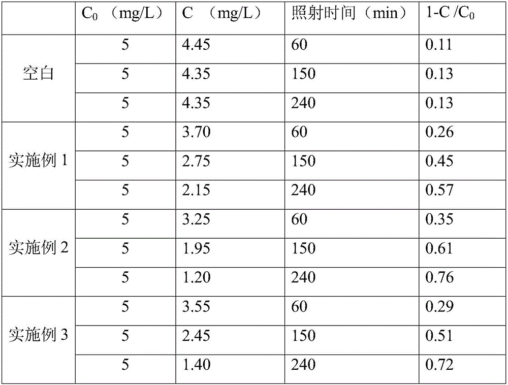
[0032] Ag, N co-doped TiO prepared in the above-mentioned Examples 1-3 2The nanometer monolayer film can be applied to the photocatalytic degradation of liquid-phase dyes.
[0033] In order to show that t...
PUM
| Property | Measurement | Unit |
|---|---|---|
| thickness | aaaaa | aaaaa |
| thickness | aaaaa | aaaaa |
| thickness | aaaaa | aaaaa |
Abstract
Description
Claims
Application Information
