Memory solder joint realizing interconnection of 3D packaging chips

A technology for chip mounting and memory, applied in the field of three-dimensional packaging of electronic devices, to achieve the effect of high service life and high reliability requirements

Active Publication Date: 2015-10-14
XUZHOU NORMAL UNIVERSITY
View PDF6 Cites 3 Cited by
  • Summary
  • Abstract
  • Description
  • Claims
  • Application Information

AI Technical Summary

Problems solved by technology

[0004] At present, the industry still lacks high-reliability interconnection solder joints that can

Method used


Image

  • Memory solder joint realizing interconnection of 3D packaging chips
  • Memory solder joint realizing interconnection of 3D packaging chips
  • Memory solder joint realizing interconnection of 3D packaging chips

Examples


Embodiment 1

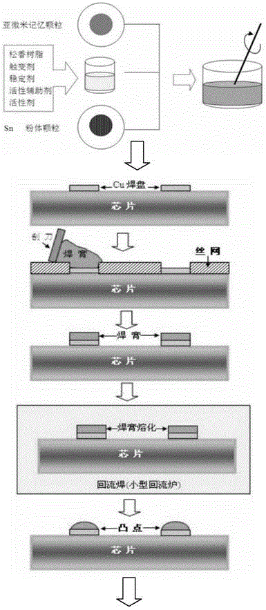
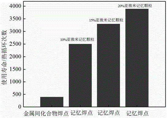
[0016] The solder paste containing submicron memory particles used for interconnection of 3D packaged chips has a submicron memory particle content of 10%, and the balance is Sn. Mix rosin resin, thixotropic agent, stabilizer, active auxiliary and active agent to prepare solder paste.

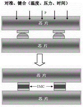
[0017] The service life of the memory solder joint formed after bonding (235℃, 9MPa) is about 2500 thermal cycles (taking into account the test error), and the solder paste has excellent solderability.

Embodiment 2

[0019] The solder paste containing sub-micron memory particles used for interconnection of 3D packaged chips has a sub-micron memory particle content of 12%, and the balance is Sn. Mix rosin resin, thixotropic agent, stabilizer, active auxiliary and active agent to prepare solder paste.

[0020] The service life of the memory solder joint formed after bonding (255℃, 5MPa) is about 2850 thermal cycles (taking into account the test error), and the solder paste has excellent solderability.

Embodiment 3

[0022] The solder paste containing sub-micron memory particles used for interconnection of 3D packaged chips has a sub-micron memory particle content of 14%, and the balance is Sn. Mix rosin resin, thixotropic agent, stabilizer, active auxiliary and active agent to prepare solder paste.

[0023] The service life of the memory solder joint formed after bonding (245℃, 10MPa) is about 3000 thermal cycles (taking into account the test error), and the solder paste has excellent solderability.


PUM


Abstract

The present invention discloses a memory solder joint realizing interconnection of 3D packaging chips and belongs to the field of three-dimensional packaging of electronic devices. The memory solder joint is prepared by the following steps: preparing pasty memory-alloy-particle-containing solder paste by using marketed Sn powder, mixed rosin resin, a thixotropic agent, a stabilizer, an activity adjuvant, an active agent and submicron CuZnAl memory alloy particles; preparing salient points on the surfaces of the chips by adopting the precision screen printing and reflow processes; and realizing vertical stacking interconnection of the chips at a certain pressure (5-10Mpa) and at the temperature (235-255 DEG C).

Description

Technical field [0001] The invention relates to a memory solder joint for realizing the interconnection of a 3D packaged chip, belonging to the field of three-dimensional packaging of electronic devices, and a high-performance interconnect solder joint. The memory solder joints are mainly used for high-reliability interconnection solder joints for chip vertical stacking. Background technique [0002] Three-dimensional (3D) packaging technology continues the application of Moore's Law and has become an important research topic in the electronics industry. 3D packaging is known as a new generation of packaging technology. The development of this technology has directly turned electronic packaging from the 2D plane of the chip to the 3D space, and the vertical stacking interconnection technology between the chips has also become an important research topic in the 3D space. [0003] In order to achieve a vertical stack of interconnect chips, using the industry made solid - liquid inte...

Claims


Application Information

Patent Timeline
IPC IPC(8): H01L23/488H01L21/60
Inventor 张亮孙磊郭永环
Owner XUZHOU NORMAL UNIVERSITY
Why Eureka
Try Eureka