Light emitting diode epitaxial wafer and manufacturing method therefor

A technology of light-emitting diodes and epitaxial wafers, which is applied in the direction of electrical components, circuits, semiconductor devices, etc., can solve the problems of insufficient current expansion of epitaxial wafers, and achieve the effects of avoiding lattice mismatch, improving crystal quality, and reducing defects

Active Publication Date: 2015-10-21
HC SEMITEK SUZHOU
View PDF3 Cites 7 Cited by
  • Summary
  • Abstract
  • Description
  • Claims
  • Application Information

AI Technical Summary

Problems solved by technology

[0006] In order to solve the problem of insufficient current expansion of epitaxial wafers in the prior art, an embodiment of the present invention provides a light-emitting diode epitaxial wafer and a manufacturing method thereof

Method used


Image

  • Light emitting diode epitaxial wafer and manufacturing method therefor
  • Light emitting diode epitaxial wafer and manufacturing method therefor

Examples


Embodiment Construction

[0024] In order to make the object, technical solution and advantages of the present invention clearer, the implementation manner of the present invention will be further described in detail below in conjunction with the accompanying drawings.

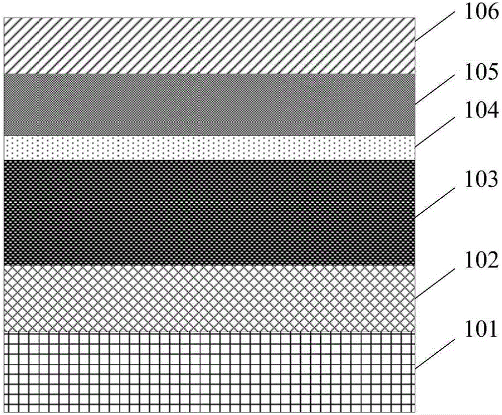
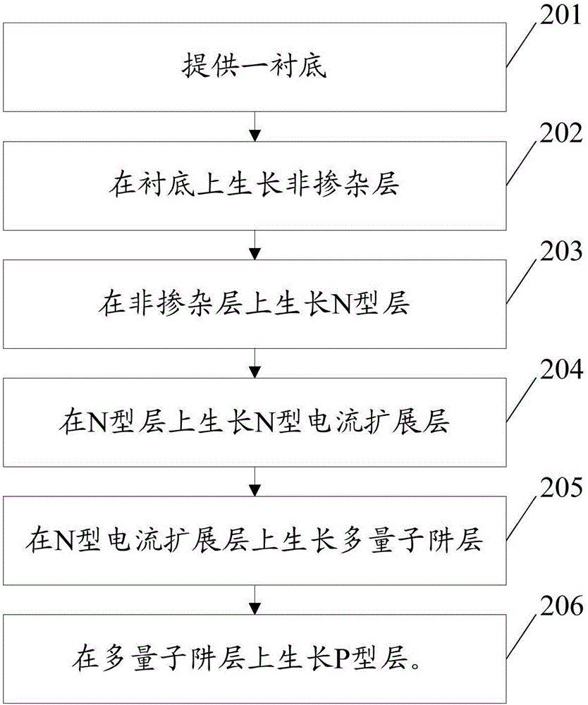
[0025] figure 1 is a schematic structural view of a light-emitting diode epitaxial wafer provided by an embodiment of the present invention, see figure 1 The light emitting diode epitaxial wafer includes a substrate 101 , an undoped layer 102 , an N-type layer 103 , an N-type current spreading layer 104 , a multi-quantum well layer 105 and a P-type layer 106 sequentially formed on the substrate 101 .

[0026] The N-type current spreading layer 104 includes an AlGaN / n-GaN superlattice structure, and the Al content of the AlGaN sublayer in the AlGaN / n-GaN superlattice structure increases layer by layer along the growth direction of the epitaxial wafer, The content of Al in the AlGaN sub-layer is 10%-80%.

[0027] Wherein, the AlGaN sub...


PUM


Abstract

The invention discloses a light emitting diode epitaxial wafer and a manufacturing method therefor and belongs to the field of light emitting diodes. The light emitting diode epitaxial wafer comprises a substrate, and a non-doped layer, an N-type layer, an N-type current expansion layer, a multi-quantum well layer and a P-type layer which are formed on the substrate in sequence. The N-type current expansion layer comprises an AlGaN/n-GaN superlattice structure. The content of Al in an AlGaN sublayer of the AlGaN/n-GaN superlattice structure is increased layer by layer in the growth direction of the epitaxial wafer and is from 10% to 80%.

Description

technical field [0001] The invention relates to the field of light-emitting diodes, in particular to a light-emitting diode epitaxial wafer and a manufacturing method thereof. Background technique [0002] As a very influential new product in the optoelectronics industry, LED has the characteristics of small size, long service life, colorful colors, and low energy consumption. It is widely used in lighting, display screens, signal lights, backlights, toys and other fields. Generally, LEDs are mainly composed of brackets, silver glue, chips, gold wires and epoxy resin. Among them, the chip is the core component of the LED, which is processed by epitaxial wafers through multiple processes. Therefore, the structure of the epitaxial wafer determines the quality of the LED. [0003] The traditional GaN-based epitaxial wafer growth method is to grow an undoped GaN layer, an N-type layer, a multi-quantum well layer and a P-type layer sequentially on the substrate layer. Among th...

Claims


Application Information

Patent Timeline
Patent Type & Authority Applications(China)
IPC IPC(8): H01L33/04H01L33/06H01L33/14H01L33/00
CPCH01L33/007H01L33/04H01L33/06H01L33/14
Inventor 李昱桦乔楠陈柏松胡加辉魏世祯
Owner HC SEMITEK SUZHOU
Why Eureka
Try Eureka