Light emitting diode chip and light emitting diode package

A technology of light-emitting diodes and diode parts, which is applied in the direction of electrical components, electric solid-state devices, circuits, etc., can solve the problem of unprovided yield and other problems, and achieve the effect of preventing the reduction of light-emitting area, high resistance, and size reduction

Active Publication Date: 2018-09-07
SEOUL VIOSYS CO LTD
View PDF10 Cites 0 Cited by
  • Summary
  • Abstract
  • Description
  • Claims
  • Application Information

AI Technical Summary

Problems solved by technology

However, this technique still does not provide good yield

Method used


Image

  • Light emitting diode chip and light emitting diode package
  • Light emitting diode chip and light emitting diode package
  • Light emitting diode chip and light emitting diode package

Examples


Embodiment Construction

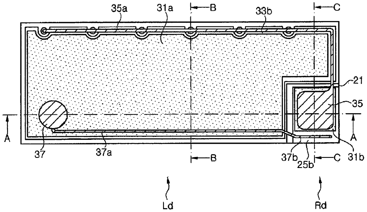
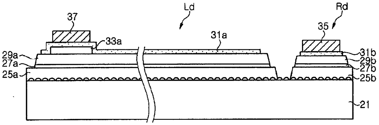
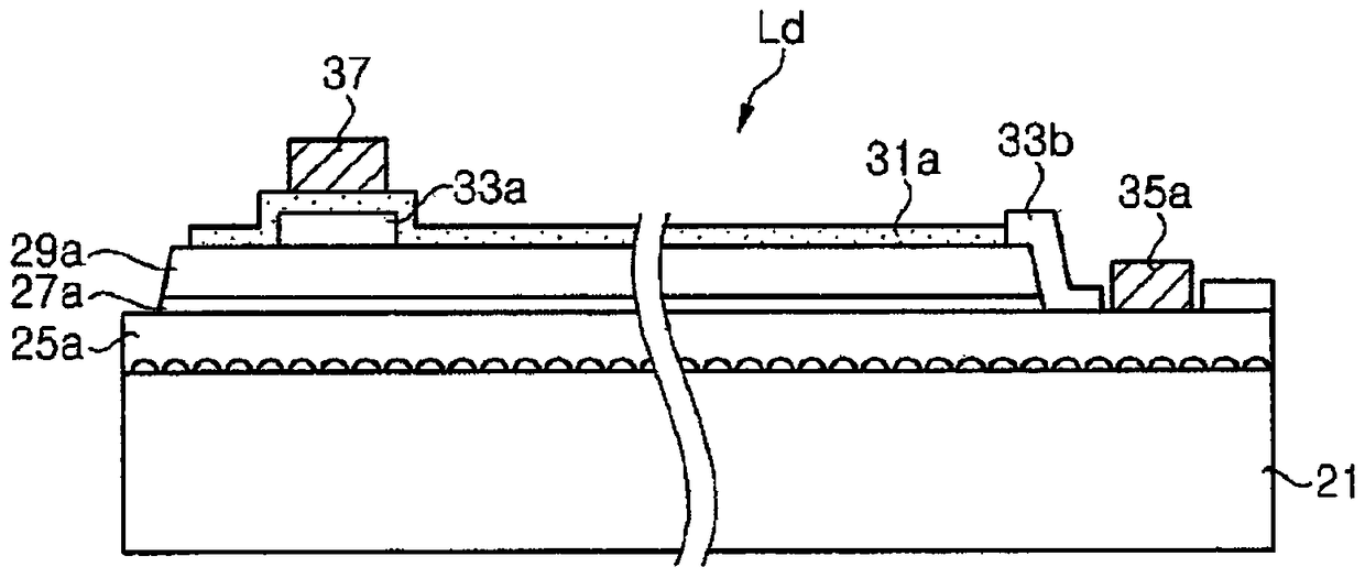
[0056] The present invention will be described more fully hereinafter with reference to the accompanying drawings that show typical embodiments of the invention. However, this invention can be embodied in many different forms and should not be construed as limited to the exemplary embodiments set forth herein. Rather, these exemplary embodiments are provided so that the disclosure of the present invention will be complete and will fully convey the concept of the present invention to anyone who has ordinary knowledge in the technical field to which the present invention pertains. Also, it should be noted that the drawings are not drawn in exact scale, and certain dimensions in the drawings, such as width, length, thickness, etc., may be exaggerated for clarity. In this specification, the same elements are denoted by the same reference numerals.

[0057] It should be understood that when an element or layer is referred to as being "on" or "connected to" another element or layer...


PUM


Abstract

The present invention provides a light emitting diode chip and a light emitting diode package including the same. The light emitting diode chip includes a substrate, a light emitting diode section disposed on the substrate, an inverse parallel diode section disposed on the substrate and connected inversely parallel to the light emitting diode section. In the light emitting diode chip, the light emitting diode section is disposed together with the inverse parallel diode section.

Description

technical field [0001] Typical embodiments of the present invention relate to a light emitting device, and more particularly to a light emitting diode chip and a light emitting diode package that are resistant to electrostatic discharge. Background technique [0002] Generally, GaN-based compound semiconductors are formed by epitaxial growth on a sapphire substrate having a similar crystal structure and lattice parameters to reduce lattice defects. However, the epitaxial layer grown on the sapphire substrate may have many types of crystal defects, such as V-fits, threading dislocation, and the like. When a high-voltage static electricity is applied to the LED from the outside, the current will concentrate on the crystal defects in the epitaxial layer, thus causing the breakdown of the diode. [0003] Recently, the number of applications of high-brightness / high-output light-emitting diodes (LEDs) has increased, not only for backlight units of light-emitting diode televisions...

Claims


Application Information

Patent Timeline
Patent Type & Authority Patents(China)
IPC IPC(8): H01L33/36H01L33/62H01L33/46
CPCH01L2224/48091H01L2224/48247H01L2224/48257H01L2924/181H01L2924/00014H01L2924/00012
Inventor 徐德壹金京完尹馀镇禹尙沅金信亨
Owner SEOUL VIOSYS CO LTD
Why Eureka
Try Eureka