On-board nand FLASH bad area management system

A technology for managing systems and bad areas, which is applied in the field of satellite detection data access to achieve the effects of improving use efficiency, realizing large-capacity data access, and ensuring correctness and integrity

Active Publication Date: 2018-05-22
SHANGHAI SATELLITE ENG INST
View PDF3 Cites 0 Cited by
  • Summary
  • Abstract
  • Description
  • Claims
  • Application Information

AI Technical Summary

Problems solved by technology

However, due to the process structure of the NAND FLASH chip, some bad areas will appear during use, and the stand-alone machine must have the function of updating the bad area table in real time

Method used


Image

  • On-board nand FLASH bad area management system
  • On-board nand FLASH bad area management system

Examples


Embodiment Construction

[0024] The present invention will be described in detail below in conjunction with specific embodiments. The following examples will help those skilled in the art to further understand the present invention, but do not limit the present invention in any form. It should be noted that those skilled in the art can make several changes and improvements without departing from the concept of the present invention. These all belong to the protection scope of the present invention.

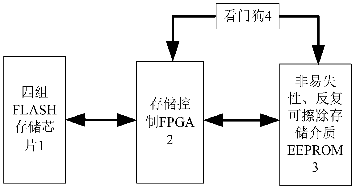
[0025] The invention relates to the design of bad area management of on-board solid storage, and the solid storage refers to solid state storage or solid state memory.

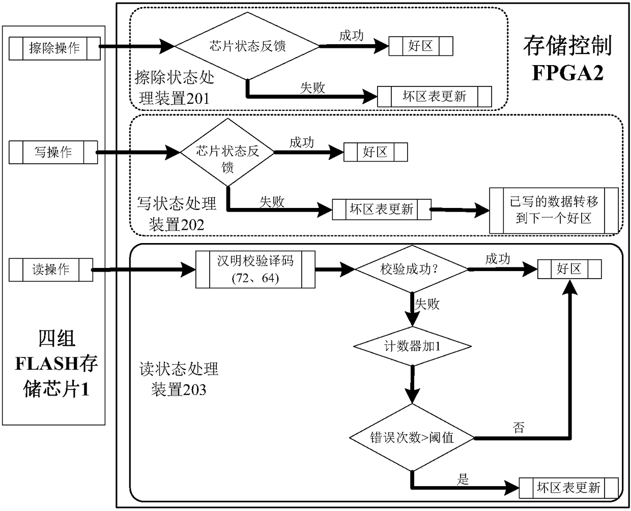
[0026] The on-board NAND FLASH solid storage bad area management system includes devices: four groups of FLASH memory chips 1, used for recording and replaying satellite load detection data, providing chip status feedback information during the solid storage erasing and writing process, and Fixedly store the verification information whe...


PUM


Abstract

The present invention provides a management system for satellite-borne NAND FLASH solid storage bad areas, including: four groups of FLASH storage chips, used for recording and replaying satellite load detection data, and providing chip status feedback information during solid storage erasing and writing processes And verification information; storage control FPGA, used to control the erasing, writing and reading operations of the FLASH memory chip, judge the quality of the block according to the chip feedback information and verification information of the FLASH memory chip, and facilitate the EEPROM to update the bad area table; EEPROM is used to store the bad area table information of the FLASH memory chip; the watchdog is used to prevent the storage control FPGA control signal terminal from being in an uncertain state and mistakenly write error information into the EEPROM during the power-on and power-off process of the single machine. The invention can be applied to the meteorological satellite data transmission sub-system, and the bad area management method effectively guarantees the correctness and integrity of the satellite on-orbit remote sensing data.

Description

technical field [0001] The invention relates to the field of satellite detection data access, in particular to the design of a satellite-borne NAND FLASH solid storage bad area management system. Background technique [0002] With the significant increase in the input rate of satellite loads, the demand for solid storage capacity has increased significantly, and the memory chips have been replaced by NAND FLASH series chips from SDRAM type. The memory capacity of the chip is 32Gbits. The newly adopted memory chip has the characteristics of high integration, the indicators meet the application requirements, the technology is relatively mature, and it has the experience of in-orbit flight verification. [0003] When used on a satellite, the storage module is composed of an ACTEL FPGA A54SX32A plus a NAND FLASH chipset, and uses (72, 64) Hamming check to enhance the anti-single event flipping capability of the FLASH storage board. One of the memory chips is used for EDAC verif...

Claims


Application Information

Patent Timeline
Patent Type & Authority Patents(China)
IPC IPC(8): G06F3/06
Inventor 刘波张恒刘辉郑莲玉
Owner SHANGHAI SATELLITE ENG INST
Why Eureka
Try Eureka