MEMS switch with internal conductive path
A technology of conductive channels and inner conductors, applied in the field of MEMS switches, can solve problems such as increasing the risk of short circuit in the expected closed circuit
- Summary
- Abstract
- Description
- Claims
- Application Information
AI Technical Summary
Problems solved by technology
Method used
Image
Examples
Embodiment Construction
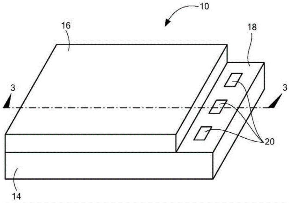
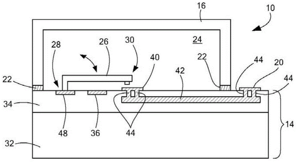
[0022] In an illustrative embodiment, a MEMS switch within a wafer-level package more efficiently transfers signals between its internal movable parts and external pads while reducing shorting to its lid. To this end, MEMS switches are formed on a chip with internal conductors electrically connected between the movable part and external pads. One or more vias extending from the device surface to the internal conductors reduce signal impedance, thereby increasing efficiency. Furthermore, the insulating material between the inner conductor and the adhesive material connecting the cover to the switch chip reduces short circuits to its cover through the adhesive material. Details of illustrative embodiments are discussed below.
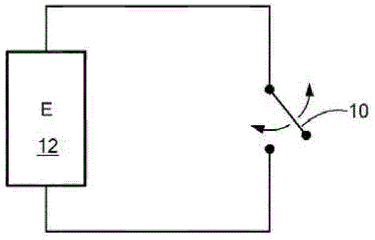
[0023] figure 1 A circuit that may use a MEMS switch 10 configured in accordance with an illustrative embodiment of the invention is schematically shown. In fact, the figure shows a very simplified circuit in which the MEMS switch 10 can open and close...
PUM
 Abstract
Description
Claims
Application Information
 - R&D
- Intellectual Property
- Life Sciences
- Materials
- Tech Scout
- Unparalleled Data Quality
- Higher Quality Content
- 60% Fewer Hallucinations
Browse by: Latest US Patents, China's latest patents, Technical Efficacy Thesaurus, Application Domain, Technology Topic, Popular Technical Reports.
© 2025 PatSnap. All rights reserved.Legal|Privacy policy|Modern Slavery Act Transparency Statement|Sitemap|About US| Contact US: help@patsnap.com


